T7-X Series Modules
This topic describes information about implementing serial communication between T7-X series modules and MCUs.
Overview
T7-X series modules, including T7-U, T7-U-IPEX, T7-2S, and T7-M, are embedded dual-band 2.4 GHz & 5 GHz Wi-Fi and Bluetooth combo modules with low power consumption. They support the access point (AP) mode and station (STA) mode for Wi-Fi connection, as well as a connection over Bluetooth Low Energy (BLE).
Serial protocol
Serial communication between module and MCU
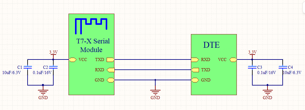
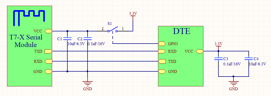
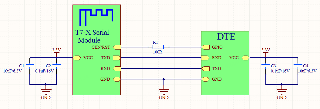
- Connection between a module and a 3.3V MCU
-
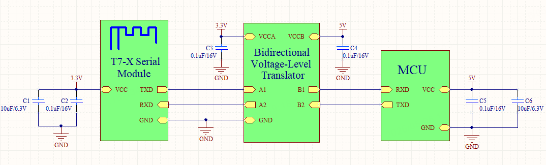
Connection between a module and a 5V MCU
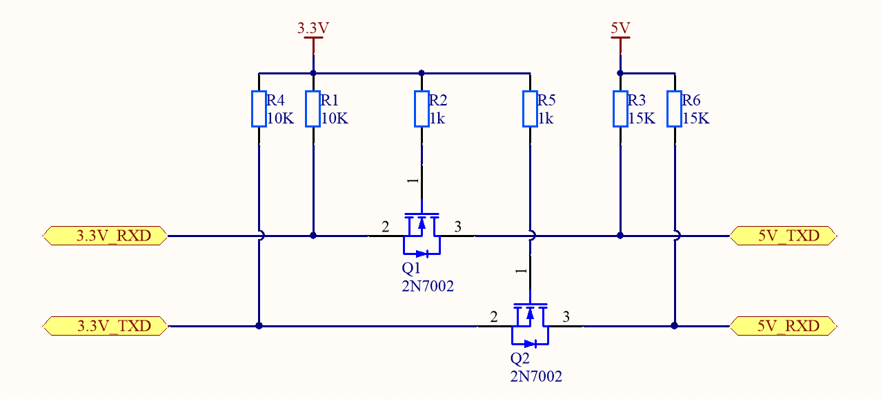
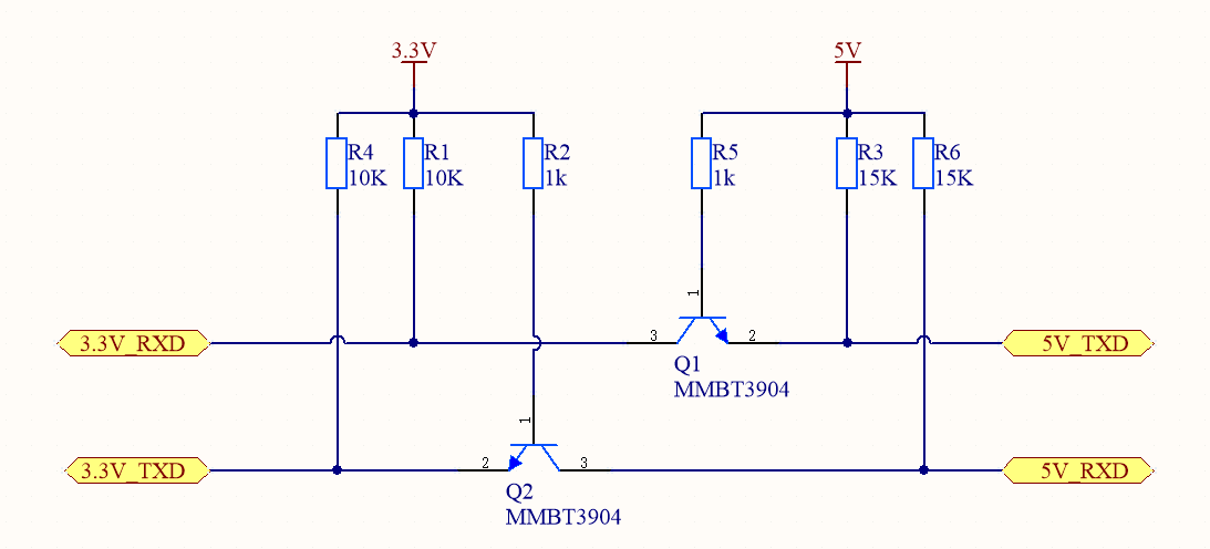
In the following circuit diagram, voltage level translation can be implemented with a bidirectional level-shifter IC, a MOSFET circuit, or a transistor circuit.
Level translator reference
- N-channel MOSFET level translator: An N-channel MOSFET and a built-in body diode are used to implement two-way communication.
- NPN triode level translator: An NPN triode is used to implement one-way communication.
Design specification
Serial port pin
The following table lists the specification and pin information of T7-X modules for serial communication with an MCU.
| Module model | Input voltage (Typical) | Input current (Max) | TX pin No. | TX silk screen | RX pin No. | RX silk screen |
|---|---|---|---|---|---|---|
| T7-U | 3.3V | 500 mA | 15 | TX0 | 16 | RX0 |
| T7-U-IPEX | 3.3V | 500 mA | 15 | TX0 | 16 | RX0 |
| T7-2S | 3.3V | 500 mA | 7 | TX | 5 | RX |
| T7-M | 3.3V | 500 mA | 7 | TX0 | 5 | RX0 |
Power supply
- For modules with a 3.3 V input voltage, the supply current must be greater than the maximum input current. The total capacity of the external filter capacitor should be greater than 10 μF.
- Place the filter capacitors C1 and C2 near the power pin of the module.
Pins on module
- The CEN pin of the module is a hardware reset pin. The module has internal weak pull-up resistors configured. If the pin is not used, it can float. If a module has been paired, this pin cannot be used to clear pairing information.
- The maximum input level of the ADC port is 3.3V. It is recommended to use MΩ-level external voltage divider resistors and place a 100 nF ground filter capacitor close to the ADC port.
- The TX1 pin is the mode selection pin. Pull it low before power-on to enter the ATE test firmware. Leave it floating or pull it high to enter the application firmware. During normal operation, this pin works as the log output port.
- Leave other unused pins floating.
- For detailed pin information, see the module datasheets.
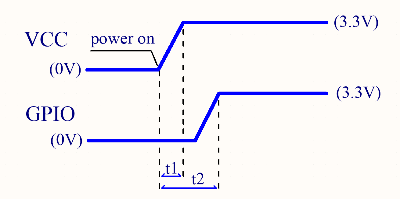
Power-on sequence of the module
Suppose that the high-level voltage settling time of the module’s GPIO is t2 and the voltage settling time of the module power pin is t1. Every time the module is powered on, t2 must be greater than or equal to t1, as shown in the following figure.
Antenna clearance
-
Do not use metal shells or plastic shells with metallic painting or coating in the direction of the antenna radiation. Do not use metal objects such as screws and rivets near the antenna, which might affect the antenna efficiency.
-
Try to increase the distance from the top shell to the antenna to minimize the impact on antenna performance.
- Try to increase the distance from the upper and bottom shells to the antenna to minimize the impact on antenna performance.
-
Keep the module away from speakers, power switches, cameras, HDMI, USB, and other high-speed signals to avoid interference.
-
Avoid metal shielding near the antenna. If co-channel interference occurs, you must evaluate the impact on the antenna performance and ensure isolation from interference.
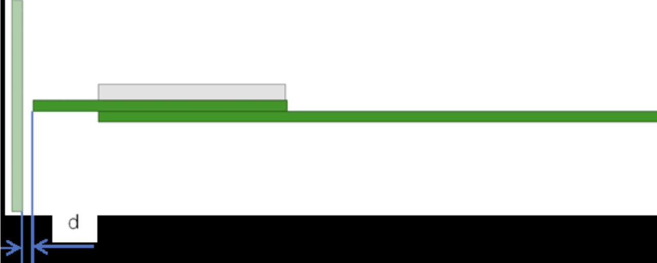
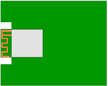
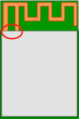
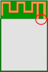
Antenna placement
-
Horizontal placement
We recommend that you place the module at the edge of the backplane with the antenna facing outward, and flush the module’s GND terminal with the backplane’s GND terminal. Both terminals are fully connected.
-
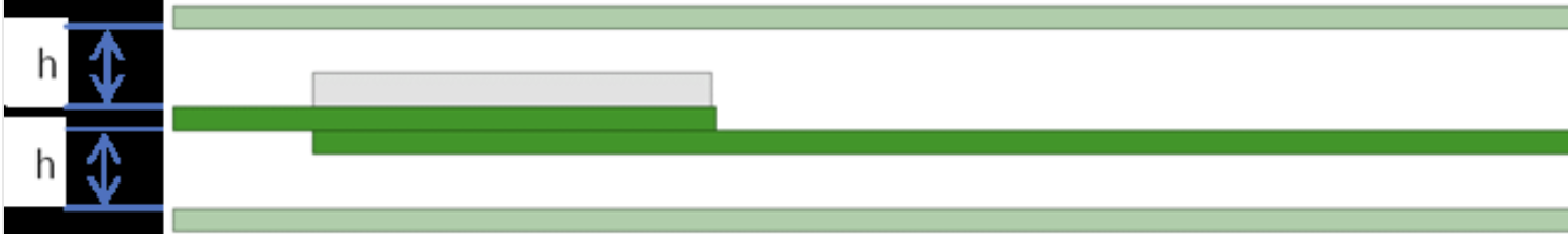
Embedded placement
-
Embed the module into the backplane through a slot that is flush with or deeper than the module’s GND terminal. The side of the slot must be 15 mm or farther from the module’s board edge.
-
A wider slot can achieve better performance that is still weaker than that of horizontal placement.
-
-
Vertical placement
Insert the module vertically into the backplane slot with the antenna facing upward. The module’s GND terminal and the backplane’s GND terminal must be fully connected. We recommend that you keep a clearance distance of 15 mm or more around the antenna.
-
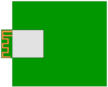
Position of the antenna on the backplane
When the MCU backplane is large, select the antenna position according to the following rules:
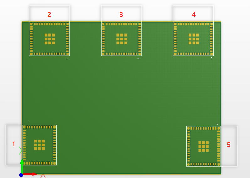
- When the antenna comes out from the left side of the module, you can choose position 1 or position 2 (optimal).
- When the antenna comes out from the right side of the module, you can choose position 5 or position 4 (optimal).
Low power design
Option 1: Control module power pin on/off
This circuit design can achieve overall low power consumption.
How it works
As shown in the circuit diagram, the MCU can control the switch S1 with the GPIO pin to power on/off the module.
- When the MCU has data to report to the cloud, it turns the
S1on. Then, the module can receive data from the MCU and report data to the cloud and the mobile app. - When data reporting is completed, the module will be powered off and consume no power.
Option 2: Reduce power consumption in the idle state
Pull down the module’s clock enable (CEN) pin or reset (RST) pin to reduce idle consumption.
How it works
As shown in the circuit diagram, the MCU can control the CEN or RST pin with the GPIO pin to power on/off the module.
- When the MCU has data to report to the cloud, the GPIO outputs high to power on the module. Then, the module can receive data from the MCU and report data to the cloud and the mobile app.
- When data reporting is completed, the GPIO outputs low and the module runs in reset mode with low power consumption.
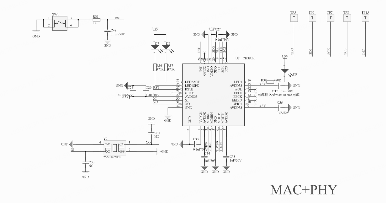
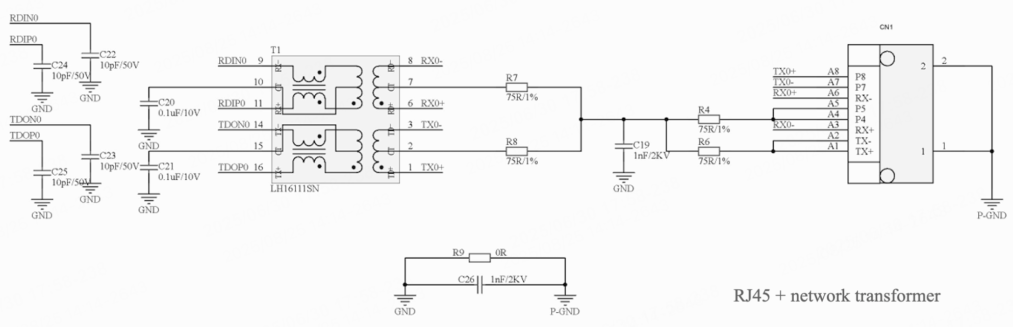
SPI to Ethernet
You can use the CH390H Ethernet transceiver chip. The schematic diagram is as follows:
Anti-interference design
Relay switching can generate arc interference. Optimize power components and relay selection as follows:
- Use high-frequency electrolytic capacitors instead of power-frequency electrolytic capacitors.
- Select EE-type inductors or I-shaped inductors with nickel-zinc magnetic cores.
- Place a ceramic capacitor of about 10 μF near the module VCC and GND pins.
For layout optimization, follow these guidelines:
- Use single-point grounding whenever possible.
- Connect each grounding wire separately to the negative terminal of the capacitor.
- Minimize high-frequency current loops.
- Keep the module away from relays and inductors.
- Place the electrolytic capacitor/metal terminal between the module and the relay/inductor to provide shielding and isolation.
Radio frequency (RF) test
Antenna performance is sensitive to nearby components and shell distance. We recommend that you test the radio frequency (RF) performance after the final test. The RF test items and metrics are listed in the following table.
| Test item | Test metric |
|---|---|
| Increasing indoor distance | ≥ 30 m |
| Increasing outdoor distance | ≥ 100 m |
| Total radiated power (TRP) in the signaling mode of end devices (test mode of 11B 11 Mbit/s) | ≥ 10 dBm |
| Total isotropic sensitivity (TIS) in the signaling mode of end devices (test mode of 11B 11 Mbit/s) | ≤ -80 dBm |
Is this page helpful?
YesFeedbackIs this page helpful?
YesFeedback


