XR1 Module
Scope of application
This topic describes relevant information about XR1 module during MCU connection development.
XR1 is a low power embedded Wi-Fi module developed by Tuya Smart. The module consists of a highly integrated radio-frequency identification (RFID) chip XR809 and a few peripheral components, with built-in Wi-Fi network protocol stack and various library functions.
XR1 has a built-in ARM Cortex-M4F CPU, 2 MB flash ROM, 384 KB static random access memory (SRAM), and rich peripheral resources. As a real time operating system (RTOS) platform, XR1 integrates all function libraries of Wi-Fi MAC and TCP/IP protocols. You can develop your own embedded Wi-Fi products.
For more information, see XR1 Module Datasheet.
Typical application diagram
Figure 1 is a reference diagram of coordinated processing mode of the module and 3.3 V MCU.
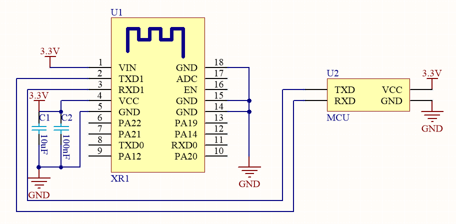
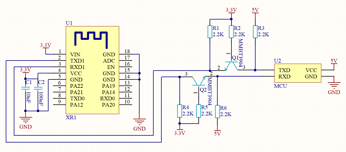
Figure 2 is a reference diagram of coordinated processing mode of the module and 5 V MCU.
Design specification
-
Module power supply:
- When the module is in the working mode, the maximum current reaches 184 mA. It is recommended that supply current of the 3.3 V module should exceed 300 mA.
- In the PCB layout, capacitors C1 and C2 at the power input pin shall be arranged near the power supply pin. The capacitance shall exceed 10 uF.
-
Module pin:
- Pin 17 (ADC) needs to float when not in use. As the ADC input port, the input voltage ranges from 0 V to 2.5 V.
- During firmware burning, pin 4 (PB02) and pin 19 (PB03) must be pulled down at the same time. When the module is working normally, they cannot be pulled down at the same time.
-
Radio frequency (RF) of the module:
-
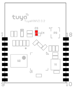
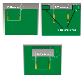
The module has two types of antennas, PCB onboard antenna and external antenna. By default, PCB onboard antenna is used. You can modify antenna connection method by switching a jumper resistor. XR1 has 0omh/0201 resistor, which is marked red in the following figure.
-
When a PCB onboard antenna is used in the Wi-Fi module, it is recommended that the distance between the module antenna and other metal parts should be at least 15 mm, in order to optimize the Wi-Fi performance. Wiring and copper pour are not allowed in the antenna area of the PCB, in order not to affect the antenna performance. Key points of layout: Make sure that no substrate medium exists directly below or above the printed antenna, and the printed antenna is away from the copper sheet. In this way, antenna radiation effect is guaranteed to the maximum extent.
-
Is this page helpful?
YesFeedbackIs this page helpful?
YesFeedback


