TYWE3S Module
Scope of application
This topic describes relevant information about TYWE3S module during MCU connection development.
TYWE3S is a low power embedded Wi-Fi module developed by Tuya Smart. The module consists of a highly integrated radio-frequency identification (RFID) chip ESP8266 and a few peripheral components, with built-in Wi-Fi network protocol stack and various library functions. TYWE3S also has a low power 32-bit CPU, 2 MB flash, 50 KB static random access memory (SRAM), and rich peripheral resources. On this basis, you can develop your own embedded Wi-Fi products. For example, build prototypes of sockets, power strips, and switches.
For more information, see TYWE3S Module Datasheet.
Typical application diagram
Figure 1 is a reference diagram of coordinated processing mode of TYWE3S module and MCU.
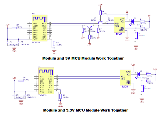
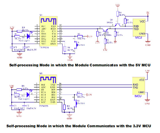
Figure 2 is a reference diagram of self-processing mode of TYWE3S module after connection with MCU.
Design specification
-
Module power supply:
- Power consumption: 3.3V/100mA. Transient (5 us) current: 450mA. Recommended supply current: ≥ 300mA.
- Power filter capacitors C1 and C2 shall be arranged near the VCC pin.
-
Module pin:
- Serial ports TXD and RXD are communication ports. During start, lots of module information data is output. Default settings are as follows. Baud: 9600, data bit: 8 bits, stop bit: 1 bit, no check bit, and no flow control.
- ADC pin is a voltage acquisition pin, and cannot be used as a general I/O port. When not in use, the pin can float.
- I/O 0 takes part in normal start of the module. During power on and start, the pin needs a high electrical level to start normally. As an output port, it is recommended to add a pull-up resistor. As an input port, consider the electrical level of the pin during power on. When not in use, the pin can float.
- I/O 2 takes part in normal start of the module. During power on and start, the pin needs a high electrical level to start normally. It is a debugging port of the module by default. Data is output during power on. It can only be used as an output port. When not in use, the pin can float.
- I/O 15 takes part in normal start of the module. During power on and start, the pin needs a low electrical level to start normally. A pull-down resistor must be added to the pin.
- RST pin can reset the module hardware when the electrical level is low. To use it, you can connect it to the I/O port of MCU directly. External circuit is not required.
- There is no pull-up resistor inside I/O 16. Pay attention to this point during use.
- If required, the module can be connected to a button and a Wi-Fi status indicator light. The button clears network information of the module. The indicator light shows the current status of the Wi-Fi module. See Figure 1 if you use coordinated processing mode of the module and MCU. See Figure 2 if you use the self-processing mode.
-
Radio frequency (RF) of the module:
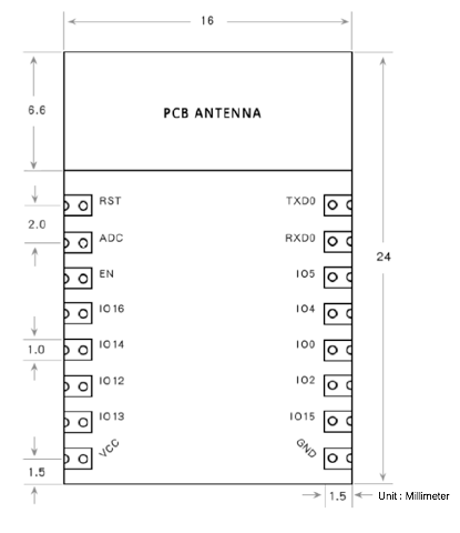
- Figure 3 is TYWE3S package diagram. ANTENNA is the antenna location. Copper pour and wiring are prohibited below this area. If the structure permits, hollow out PCB in this area, in order not to affect antenna performance.
Is this page helpful?
YesFeedbackIs this page helpful?
YesFeedback


