T34 Module Datasheet
T34 module is a Wi-Fi and Bluetooth Low Energy (LE) combo module developed by Tuya Smart. This module consists of a highly integrated wireless RF chip T34 with built-in Wi-Fi stacks and adequate library functions.
Overview
The T34 module integrates the BK7231N chip, crystal, RF matching component, and most other peripheral components. It supports both the access point (AP) mode and station (STA) mode for Wi-Fi connection as well as a connection over Bluetooth LE. This module has a built-in 32-bit MCU with a maximum running speed of 120 MHz, built-in 2 MB flash memory, 256 KB RAM, and up to six 32-bit PWM outputs. This module is ideal for high-quality LED control.
Features
- Built-in low-power 32-bit CPU that also acts as an application processor.
- Clock rate of 120 MHz.
- Operating voltage range: 3.3 ± 0.3V
- Peripherals: six PWM pins, two I2C pins, two UARTs, and one SPI.
- Wi-Fi connectivity
- IEEE 802.11b/g/n.
- Channels 1 to 14 at 2.4 GHz.
- Support security protocols including WEP, WPA/WPA2, and WPA/WPA2 PSK (AES).
- The maximum output power is +16 dBm for IEEE 802.11b transmission.
- Support STA, AP, and STA + AP combo working modes.
- Two pairing modes are supported, namely Wi-Fi Easy Connect (EZ mode) and access point (AP) mode. Both modes are suitable for pairing with Android and iOS mobile phones.
- Operating temperature range: -40°C to 105°C.
- Bluetooth LE connectivity
- The transmitter power in Bluetooth mode is 6 dBm.
- Integral Wi-Fi and Bluetooth coexistence interface.
Scope of applications
- Smart building
- Smart home and electrical appliance
- Smart socket and light
- Industrial wireless control
- Baby monitor
- IP camera
- Smart bus
Module interfaces
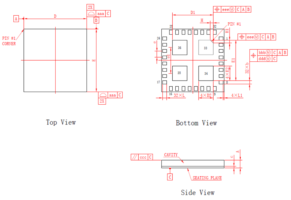
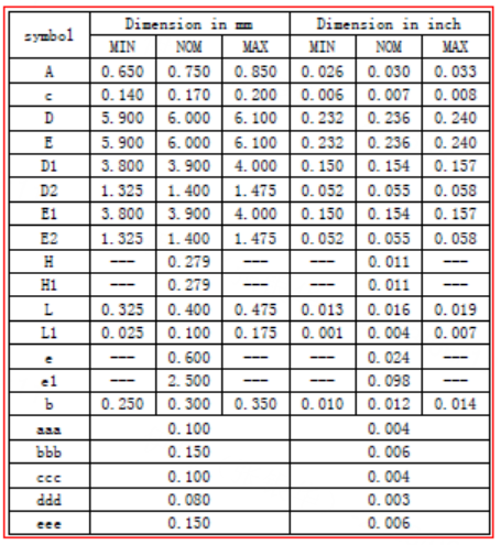
Dimensions and footprint
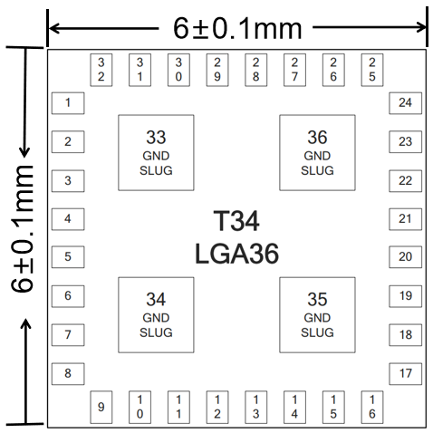
The T34 module provides 36 LGA pins. The T34 dimensions are 6±0.1 mm (W) × 6±0.1 mm (L) × 0.85±0.1 mm (H).
The following figure shows the dimensions of the T34 module.
Pin definition
| Pin No. | Symbol | I/O type | Description |
|---|---|---|---|
| 1, 3, 32, 33, 34, 35, and 36 | GND | P | Ground pins. 33, 34, 35, and 36 are the ground pads at the back of the chip. |
| 2 | ANT | I/O | External antenna with 2.4 GHz RF input and output. |
| 4 and 5 | VCCPA | P | RF PA power input. Voltage range: 3.0V to 3.6V. And 3.3V power supply is recommended. |
| 6 | VDDDIG | O | Digital power output. The voltage is about 1.2V. |
| 7 | VDDAON | O | Normally open power output. The voltage is about 1.2V. |
| 8 | VBAT | I | Chip main-power input. Voltage range: 3.0V to 3.6V. And 3.3V power supply is recommended. |
| 9 | CEN | I | The CEN pin of the chip, without a reset function. This pin is floating inside the chip. |
| 10 | P28/ADC4/RXEN | I/O | GPIO or ADC4 or set high during RF reception. |
| 11 | P14/SD_CLK/SCK/ANT0 | I/O | GPIO, or CLK of SD, or SCK of SPI, or Bluetooth LE antenna control ANT0. |
| 12 | P16/SD_CMD/MOSI/ANT2 | I/O | GPIO, or CMD of SD, or MOSI of SPI, or Bluetooth LE antenna control ANT2. |
| 13 | P15/CSN/ANT1 | I/O | GPIO, or CSN of SPI, or Bluetooth LE antenna control ANT1. |
| 14 | P17/SD_D0/MISO/ANT3 | I/O | GPIO, or D0 of SD, or MISO of SPI, or Bluetooth LE antenna control ANT3. |
| 15 | P26/ADC1/IRDA/PWM5 | I/O | GPIO, or ADC1, or IR receiver or PWM5. |
| 16 | P24/ADC2/LPO_CLK/PWM4 | I/O | GPIO, or ADC2, or low power clock 32.768K output, or PWM4. |
| 17 | P23/ADC3/TDO/F_SO | I/O | GPIO, or ADC3, or JTAG TDO, or flash data output when downloading with SPI. |
| 18 | P22/ADC5/CLK_26M/TDI/TXEN/F_SI | I/O | GPIO, or ADC5, or crystal frequency output, or JTAG TDI, or set high during RF transmission, or flash data input when downloading with SPI. |
| 19 | P21/ADC6/I2C1_SDA/TMS/F_CSN | I/O | Mode selection pin for selecting RF test firmware or app firmware. Pulling down this pin will enter the RF test mode. |
| 20 | P20/I2C1_SCL/TCK/F_SCK | I/O | GPIO, or SCL of I2C1, or TCK of JTAG, or the clock when flash is downloaded by SPI. |
| 21 | P6/CLK13M/PWM0 | I/O | GPIO, or 1, 2, 4, and 8 frequency division output of crystal clock, or PWM0. |
| 22 | P7/WIFI_ACTIVE/PWM1 | I/O | GPIO, or WIFI_ACTIVE control when Wi-Fi and Bluetooth coexist, or PWM1. |
| 23 | P8/BT_ACTIVE/PWM2 | I/O | GPIO, or BT_ACTIVE control when Wi-Fi and Bluetooth coexist, or PWM2. |
| 24 | P9/BT_PRIORITY/PWM3 | I/O | GPIO, or BT_PRIORITY control when Wi-Fi and Bluetooth coexist, or PWM3. |
| 25 | P10/DL_RX/UART1_RXD | I/O | GPIO, or RXD when downloading flash with UART, or RXD of serial port UART1. |
| 26 | P11/DL_TX/UART1_TXD | I/O | GPIO, or TXD when downloading flash with UART, or TXD of serial port UART1. |
| 27 | P1/UART2_RXD/I2C2_SDA | I/O | GPIO, or RXD of serial port UART2, or SDA of I2C2. P1 is used for self-calibration and cannot be used for other functions. |
| 28 | P0/UART2_TXD/I2C2_SCL | I/O | GPIO, or TXD of serial port UART2, or SCL of I2C2. |
| 29 | XI | I | T34 has a built-in crystal, and no external crystal is required. |
| 30 | XO | O | T34 has a built-in crystal, and no external crystal is required. |
| 31 | VSYS | O | System power output. Voltage range: 2.7V to 3.0V. |
P indicates the power pin, and I/O indicates the input and output pin.
Electrical parameters
Absolute electrical parameters
| Parameter | Description | Min value | Max value | Unit |
|---|---|---|---|---|
| Ts | Storage temperature | -55 | 125 | °C |
| VBAT | Supply voltage | -0.3 | 3.9 | V |
| Electrostatic discharge voltage (human body model) | TAMB -25°C | -4 | 4 | kV |
| Electrostatic discharge voltage (machine model) | TAMB -25°C | -200 | 200 | V |
Normal operating conditions
| Parameter | Description | Min value | Typical value | Max value | Unit |
|---|---|---|---|---|---|
| Ta | Operating temperature | -40 | - | 105 | °C |
| VBAT | Supply voltage | 3.0 | 3.3 | 3.6 | V |
| VIL | I/O low-level input | -0.3 | - | VCC × 0.25 | V |
| VIH | I/O high-level input | VCC × 0.75 | - | VCC | V |
| VOL | I/O low-level output | VSS | - | VSS + 0.3 | V |
| VOH | I/O high-level output | VCC - 0.3 | - | VCC | V |
| Imax | I/O drive current | - | 6 | 20 | mA |
| θ | Power supply slope | 100 | - | - | mV/ms |
Radio frequency (RF) power
| Working status | Mode | Rate | Transmit/Receive power | Average value | Peak (Typical) value | Unit |
|---|---|---|---|---|---|---|
| Transmit | 11b | 11 Mbit/s | +16 dBm | 280 | 304 | mA |
| Transmit | 11g | 54 Mbit/s | +15 dBm | 257 | 306 | mA |
| Transmit | 11n | MCS7 | +14 dBm | 260 | 281 | mA |
| Receive | 11b | 11 Mbit/s | Continuous reception | 75 | 85 | mA |
| Receive | 11g | 54 Mbit/s | Continuous reception | 75 | 85 | mA |
| Receive | 11n | MCS7 | Continuous reception | 77 | 85 | mA |
Operating current
| Work mode | Status (Ta = 25°C) | Average value | Peak (Typical) value | Unit |
|---|---|---|---|---|
| Quick pairing (Bluetooth) | The module is in EZ mode. The Wi-Fi network status indicator blinks quickly. | 88 | 383 | mA |
| Quick pairing (AP) | The module is in AP mode. The Wi-Fi network status indicator blinks slowly. | 85 | 300 | mA |
| Quick pairing (EZ) | The module is in EZ mode. The Wi-Fi network status indicator blinks quickly. | 90 | 378 | mA |
| Connected | The module is connected to the cloud. The Wi-Fi network status indicator is steady on. | 85 | 350 | mA |
| Disconnected | The module is disconnected from the cloud. The Wi-Fi network status indicator is steady off. | 70 | 280 | mA |
RF parameters
Basic RF features
| Parameter | Description |
|---|---|
| Operating frequency | 2.412 to 2.484 GHz |
| Wi-Fi standard | IEEE 802.11b/g/n (channels 1–14) |
| Data transmission rate | 11b: 1, 2, 5.5, and 11 Mbit/s 11g: 6, 9, 12, 18, 24, 36, 48, and 54 Mbit/s 11n: HT20 MCS0–7 11n: HT40 MCS0–7 |
| Antenna type | Onboard PCB antenna, FPC antenna, or ceramic antenna |
Wi-Fi transmitter (TX) performance
| Parameter | Min value | Typical value | Max value | Unit |
|---|---|---|---|---|
| RF average output power, 802.11b CCK mode, 11M | - | 16 | - | dBm |
| RF average output power, 802.11g OFDM mode, 54M | - | 15 | - | dBm |
| RF average output power, 802.11n OFDM mode, MCS7 | - | 14 | - | dBm |
| Frequency error | -20 | - | 20 | ppm |
Wi-Fi receiver (RX) performance
| Parameter | Min value | Typical value | Max value | Unit |
|---|---|---|---|---|
| PER < 8%, RX sensitivity, 802.11b DSSS mode, 1M | - | -88 | - | dBm |
| PER < 10%, RX sensitivity, 802.11g OFDM mode, 54M | - | -74 | - | dBm |
| PER < 10%, RX sensitivity, 802.11g OFDM mode, MCS7 | - | -72 | - | dBm |
| PER < 10%, RX sensitivity, Bluetooth LE, 1M | - | -93 | - | dBm |
Bluetooth LE TX performance
| Parameter | Min value | Typical value | Max value | Unit |
|---|---|---|---|---|
| Operating frequency | 2402 | - | 2480 | MHz |
| Transmission rate over the air | - | 1 | - | Mbit/s |
| Transmission power | -20 | 6 | 20 | dBm |
| Frequency error | -150 | - | 150 | kHz |
Bluetooth LE RX performance
| Parameter | Min value | Typical value | Max value | Unit |
|---|---|---|---|---|
| RX sensitivity | - | -93 | - | dBm |
| Max RF signal input | -10 | - | - | dBm |
| Intermodulation | - | - | -23 | dBm |
| Adjacent-channel rejection ratio | - | 10 | - | dB |
Antenna information
Antenna type
You can choose the desired T34 antenna type according to the actual space environment.
Antenna interference reduction
When a PCB antenna is used on a Wi-Fi module, we recommend that the module antenna is at least 15 mm away from other metal components. This can optimize the Wi-Fi performance. Make sure that the enclosure surrounding the antenna is not traced or filled with copper. Otherwise, the RF performance might be degraded.
Packing and production instructions
Mechanical dimensions
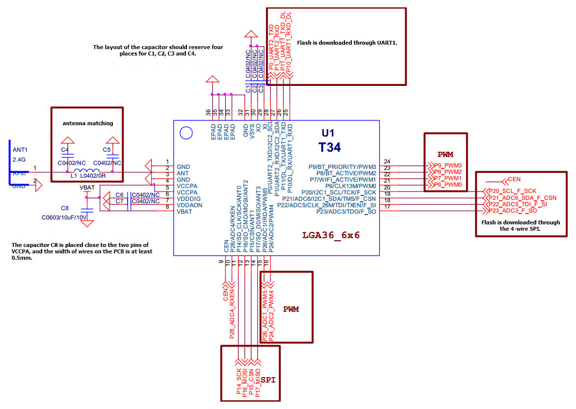
Schematic diagram
Production instructions
-
Package the module with the SMT if Tuya’s module is designed to be SMT-packaged. After being unpacked, the module must be soldered within 24 hours. Otherwise, it needs to be put into a drying cupboard with a relative humidity level no greater than 10%, or pack the module in vacuum again. Then, record the packing time and duration of exposure. The total exposure time cannot exceed 168 hours.
- Instruments or devices required for the SMT process:
- Surface mount system
- SPI
- Reflow soldering machine
- Thermal profiler
- AOI
- Instruments or devices required for the baking process:
- Cabinet oven
- Anti-electrostatic and heat-resistant trays
- Anti-electrostatic and heat-resistant gloves
- Instruments or devices required for the SMT process:
-
A delivered module must meet the following storage requirements:
-
The moisture-proof bag must be placed in an environment where the temperature is below 40°C and the relative humidity is lower than 90%.
-
The shelf life of a dry-packaged product is 12 months from the date when the product is packaged and sealed.
-
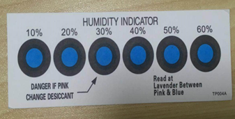
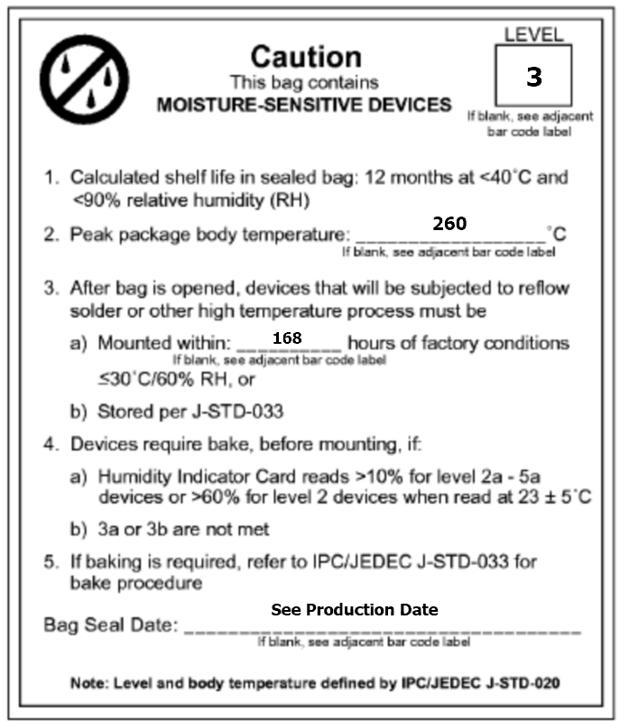
A humidity indicator card (HIC) is put in the sealed package.
-
-
The module needs to be baked in the following cases:
- The vacuum packaging bag is damaged before unpacking.
- After unpacking, no HIC is found in the packaging bag.
- After unpacking, the HIC indicates a humidity level of 10% or higher. In this case, the circle turns pink on the HIC.
- The total exposure time has lasted for over 168 hours since unpacking.
- More than 12 months have passed since the first sealing of the bag.
-
The baking parameter settings are described below:
- Baking temperature: 60°C for reel packaging with relative humidity ≤ 5%. And 125°C for tray packaging with relative humidity ≤ 5% (use the heat-resistant tray, rather than plastic containers).
- Baking time: 48 hours for reel packaging and 12 hours for tray packaging.
- Temperature for triggering an alert: 65°C for reel packaging and 135°C for tray packaging.
- Production can begin after a module has cooled down to below 36°C under natural conditions.
- If a module remains unused for over 168 hours after being baked, it needs to be baked again.
- If a batch of modules is not baked after exposure for more than 168 hours, do not use reflow soldering to solder them. Because these modules are level-3 moisture-sensitive devices, they are very likely to get damp when exposed beyond the allowable time. In this case, if they are soldered at high temperatures, device failure or poor soldering performance might occur.
-
In the whole production process, take electrostatic discharge (ESD) protective measures.
-
To guarantee the pass rate, we recommend that you use the SPI and AOI to monitor the quality of solder paste printing and mounting.
Recommended oven temperature curve
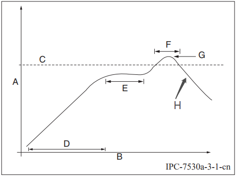
Set the temperature according to the following temperature curve of reflow soldering. The peak temperature is 245°C.
-
A: temperature axis
-
B: time axis
-
C: alloy liquidus temperature from 217°C to 220°C
-
D: ramp-up slope from 1°C/s to 3°C/s
-
E: keep a constant temperature from 150°C to 200°C for a time period from 60s to 120s
-
F: temperature above liquidus temperature for 50s to 70s
-
G: peak temperature from 235°C to 245°C
-
H: ramp-down slope from 1°C/s to 4°C/s
The curve above is based on solder paste SAC305. For more information about other solder pastes, see the recommended oven temperature curve in the specified solder paste specifications.
Storage conditions
MOQ and packaging information
| Product model | Package | Shipping packaging | MOQ |
|---|---|---|---|
| T34 | LGA36_6X6 | Tape and reel | 3,000 |
Is this page helpful?
YesFeedbackIs this page helpful?
YesFeedback


