TS24-U Module Datasheet
TS24-U is a Matter over Thread module that Tuya has developed. It consists of a highly integrated RF processing chip EFR32MG24, a few peripherals, a built-in 802.15.4 PHY/MAC Thread network protocol stack, and rich library functions.
Product overview
TS24-U is embedded with a low-power 32-bit ARM Cortex-M33 core, 1536-KB flash program memory, 192-KB RAM, and abundant peripheral resources. It integrates all function libraries of the Thread MAC and TCP/IP. You can develop embedded Thread products as required.
Features
- Embedded ARM Cortex-M 33 processor having a low-power 32-bit CPU and DSP instructions and floating-point units, which can also function as an application processor.
- Clock rate: 78 MHz
- Wide operating voltage: 2.0 to 3.8 V
- Peripherals: 9 GPIOs, 1 UART, 2 ADCs, and 5 PWMs
- Thread connectivity
- Support 802.15.4 MAC/PHY
- Working channels 11 to 26 @2.400 to 2.483 GHz, air interface rate: 250 Kbps
- Up to +10dBm output power
- 35 μA/MHz power consumption during running; 5-μA sleep current
- PCB antenna inside
- Onboard antenna with a gain of -1 dBi
- Operating temperature: -40°C to 105°C
- Support hardware encryption and AES 128/256
- Bluetooth LE radio frequency (RF) features
- Bluetooth LE
- RF data rate of up to 2 Mbit/s
- Transmitter power: +5 dBm
- Receiver sensitivity: -96 dBm@Bluetooth LE 1 Mbit/s
Applications
- Smart building
- Smart household and home appliances
- Smart socket and light
- Industrial wireless control
- Baby monitor
- Network camera
- Smart bus
Module interfaces
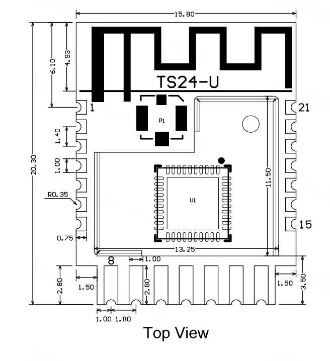
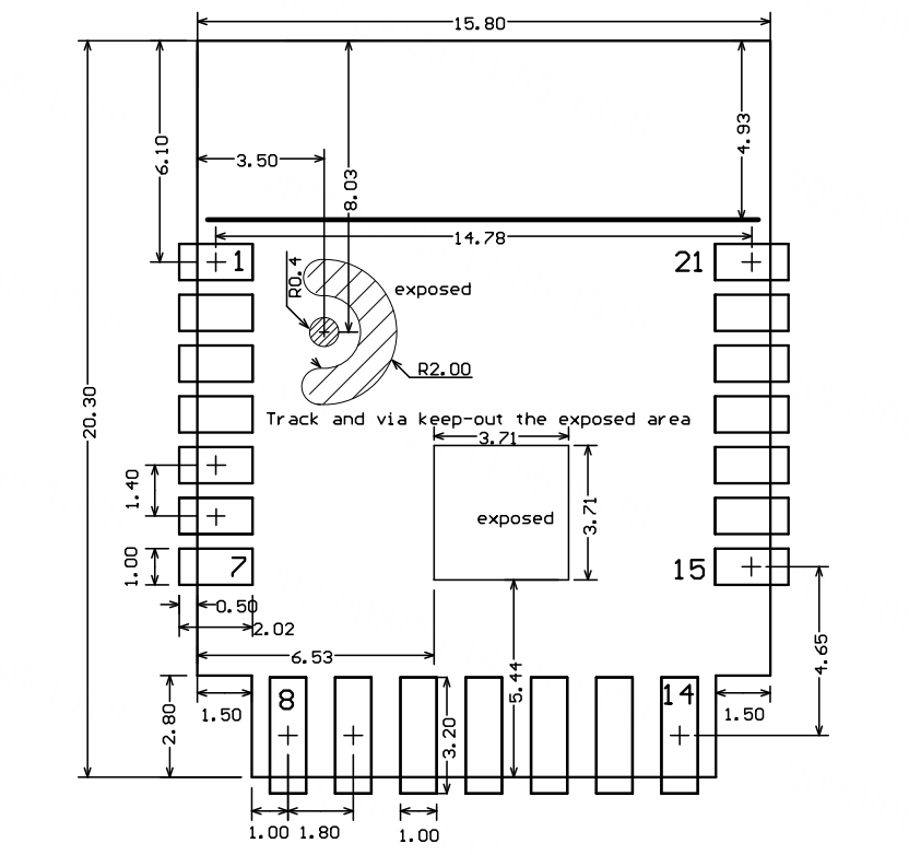
Dimensions and footprint
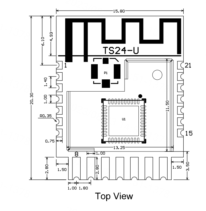
TS24-U has 3 lines of pins. The spacing of pins at the two sides is 1.4±0.1 mm, and the spacing of pins at the bottom is 1.8±0.1 mm.
The dimensions of the TS24-U are 20.3±0.35 mm (L) × 15.8±0.35 mm (W) × 3.0±0.1 mm (H).
The dimensions of TS24-U are as follows:
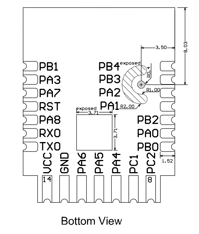
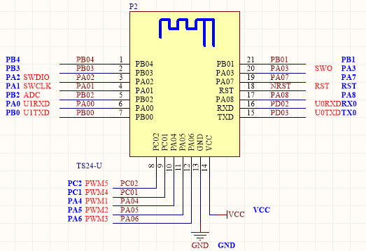
Pin definition
g)
| Pin number | Symbol | Type | Function |
|---|---|---|---|
| 1 | PB4 | I/O | Common I/O pin, which corresponds to PB04 on the internal IC |
| 2 | PB3 | I/O | Common I/O pin, which corresponds to PB03 on the internal IC |
| 3 | PA2 | I/O | Flashing pin, SWDIO, which corresponds to PA02 on the internal IC |
| 4 | PA1 | I/O | Flashing pin, SWCLK, which corresponds to PA01 on the internal IC |
| 5 | PB2 | I | ADC pin, which corresponds to PB02 on the internal IC |
| 6 | PA0 | I/O | Common I/O pin, which corresponds to PA00 on the internal IC and sends user data in low power solutions |
| 7 | PB0 | I/O | Common I/O pin, which corresponds to PB00 on the internal IC and receives user data in low power solutions |
| 8 | PC2 | I/O | Support hardware PWM and correspond to PC02 on the internal IC |
| 9 | PC1 | I/O | Support hardware PWM and correspond to PC01 on the internal IC |
| 10 | PA4 | I/O | Support hardware PWM and correspond to PA04 on the internal IC |
| 11 | PA5 | I/O | Support hardware PWM and correspond to PA05 on the internal IC |
| 12 | PA6 | I/O | Support hardware PWM and correspond to PA06 on the internal IC |
| 13 | GND | P | Power supply reference ground |
| 14 | VCC | P | Power supply pin (3.3V) |
| 15 | TX0 | I/O | UART_TXD0, used for transmitting user data and flashing authorization, which corresponds to PD03 on the internal IC |
| 16 | RX0 | I/O | UART_RXD0, used for receiving user data and flashing authorization, which corresponds to PD02 on the internal IC |
| 17 | PA8 | I | ADC pin, which corresponds to PA08 on the internal IC |
| 18 | RST | I/O | Reset pin, low active, which corresponds to RESETn on the internal IC |
| 19 | PA7 | I/O | Common I/O pin, which corresponds to PA07 on the internal IC |
| 20 | PA3 | I/O | Common I/O pin, which corresponds to PA03 on the internal IC |
| 21 | PB1 | I/O | Common I/O pin, which corresponds to PB01 on the internal IC |
- P indicates a power supply pin and I/O indicates an input/output pin.
- Pin 3, 4, 13, 14, and 18 are flashing pins, which are not exposed by default. During routing, customers should bypass them.
- TX0 and RX0 are regular serial ports, while PA0 and PB0 are low power serial ports.
Electrical parameters
Absolute electrical parameters
| Parameter | Description | Minimum value | Maximum value | Unit |
|---|---|---|---|---|
| Ts | Storage temperature | -50 | 150 | °C |
| VBAT | Power supply voltage | 2.0 | 3.8 | V |
| ESD voltage (human body model) | TAMB-25℃ | - | 2 | KV |
| ESD voltage (machine model) | TAMB-25℃ | - | 0.5 | KV |
Normal working conditions
| Parameter | Description | Minimum value | Typical value | Maximum value | Unit |
|---|---|---|---|---|---|
| Ta | Operating temperature | -40 | - | 105 | °C |
| VCC | Operating voltage | 2.0 | 3.3 | 3.8 | V |
| VIL | I/O low level input | - | - | VDD*0.3 | V |
| VIH | I/O high level input | VDD*0.7 | - | - | V |
| VOL | I/O low level output | - | - | VDD*0.2 | V |
| VOH | I/O high level output | VDD*0.8 | - | - | V |
TX and RX power consumption
| Working status | Mode | Rate | Transmit power/receive | Average value | Peak value (Typical value) | Unit |
|---|---|---|---|---|---|---|
| Transmit | - | 250 Kbps | +10 dBm | 55 | 60 | mA |
| Transmit | - | 250 Kbps | +0 dBm | 22 | 24 | mA |
| Receive | - | 250Kbps | Constantly receive | 7 | 9 | mA |
Working current
| Working mode | Working status, Ta = 25°C | Average value | Maximum value (Typical value) | Unit | Remark |
|---|---|---|---|---|---|
| EZ mode | The module is in fast network connection state. | 450 | 500 | μA | Low Power Firmware |
| Connected and busy | The module is connected to the network and in running state. | 150 | 200 | μA | Low Power Firmware |
| Connected and idle | The module is connected to the network and in idle state. | 55 | 70 | μA | Low Power Firmware |
| Deep sleep mode | Deep sleep mode, reserve 192-KB flash | 5 | - | μA |
RF parameters
Basic RF features
| Zigbee parameter | Description |
|---|---|
| Working frequency | 2.405 to 2.480 GHz |
| Zigbee standard | IEEE 802.15.4 |
| Data transmission rate | 250 Kbps |
| Antenna type | PCB antenna with a gain of -1 dBi |
| Bluetooth LE Parameter | Description |
|---|---|
| Operating frequency | 2.4 GHz ISM band |
| Wireless standard | Bluetooth LE 5.3 |
| Data transmission rate | 1 Mbit/s and 2 Mbit/s |
| Antenna type | PCB antenna with a gain of -1 dBi |
TX performance
TX performance
| Zigbee parameter | Minimum value | Typical value | Maximum value | Unit |
|---|---|---|---|---|
| Output power (250Kbps) | -30 | 10 | 13 | dBm |
| Output power adjustment stepping | - | 0.5 | 1 | dBm |
| Output spectrum adjacent channel suppression | - | -31 | - | dBc |
| Frequency error | -15 | - | 15 | ppm |
| Bluetooth LE parameter | Minimum value | Typical value | Maximum value | Unit |
|---|---|---|---|---|
| RF average output power | - | 4.5 | 5 | dBm |
| Bandwidth of 20 dB modulation signal (1 Mbit/s) | - | 2500 | - | KHz |
RX performance
RX sensitivity
| Zigbee parameter | Minimum value | Typical value | Maximum value | Unit |
|---|---|---|---|---|
| PER<8%, RX sensitivity (250 Kbps) | -104 | -104 | -103 | dBm |
| Bluetooth LE parameter | Minimum value | Typical value | Maximum value | Unit |
|---|---|---|---|---|
| RX sensitivity 1 Mbit/s | - | -96 | - | dBm |
| RX sensitivity 2 Mbit/s | - | -93.5 | - | dBm |
| Frequency offset error 1 Mbit/s | -250 | - | +300 | KHz |
| Co-channel interference suppression | - | - | -10 | dB |
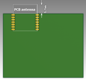
Antenna information
Antenna type
TS24-U uses the PCB antenna.
Antenna interference reduction
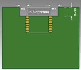
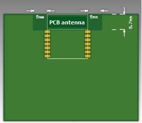
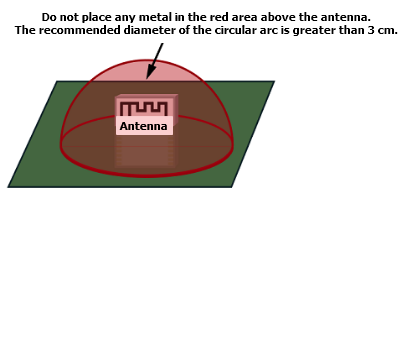
To ensure optimal RF performance when the Thread module uses a PCB antenna, it is recommended that the antenna be at least 15 mm away from other metal parts.
To prevent adverse impact on the antenna radiation performance, avoid copper or traces within the antenna area on the PCB.
Packaging information and production instructions
Mechanical dimensions
The PCB dimensions are 20.3±0.35 mm (W)×15.8±0.35 mm (L) ×1.0±0.1 mm (H).
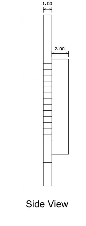
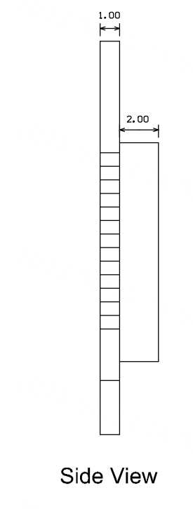
Side view
Schematic diagram of footprint
Recommended packaging
Production instructions
-
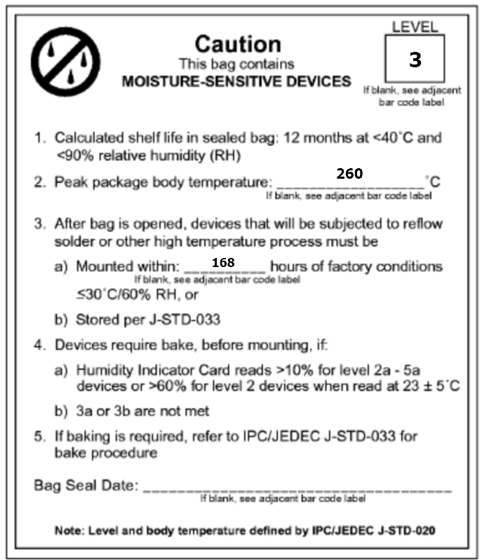
For the modules that can be packaged with the SMT or in an in-line way, you can select either of them according to the PCB design solutions of customers. If a PCB is designed to be SMT-packaged, package the module with the SMT. If a PCB is designed to be in-line-packaged, package the module in an in-line way. After being unpacked, the module must be soldered within 24 hours. Otherwise, it needs to be put into the drying cupboard where the relative humidity is not greater than 10%; or it needs to be packaged again under vacuum and the exposure time needs to be recorded (the total exposure time cannot exceed 168 hours).
- (SMT process) SMT devices:
- Mounter
- SPI
- Reflow soldering machine
- Thermal profiler
- Automated optical inspection (AOI) equipment
- (Wave soldering process) Wave soldering devices
- Wave soldering equipment
- Wave soldering fixture
- Constant-temperature soldering iron
- Tin bar, tin wire, and flux
- Thermal profiler
- Baking devices:
- Cabinet oven
- Anti-electrostatic and heat-resistant trays
- Anti-electrostatic and heat-resistant gloves
- (SMT process) SMT devices:
-
Storage conditions for a delivered module:
-
The moisture-proof bag must be placed in an environment in which the temperature is below 40°C and the relative humidity is lower than 90%.
-
The shelf life of a dry-packaged product is 12 months from the date when the product is packaged and sealed.
-
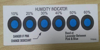
There is a humidity indicator card (HIC) in the packaging bag.
-
-
The module needs to be baked in the following cases:
- The packaging bag is damaged before unpacking.
- There is no humidity indicator card (HIC) in the packaging bag.
- After unpacking, circles of 10% and above on the HIC become pink.
- The total exposure time has lasted for over 168 hours since unpacking.
- More than 12 months have passed since the sealing of the bag.
-
Baking settings:
- Temperature: 40°C and ≤ 5% RH for reel package and 125°C and ≤5% RH for tray package (please use the heat-resistant tray rather than plastic container)
- Time: 168 hours for reel package and 12 hours for tray package
- Alarm temperature: 50°C for reel package and 135°C for tray package
- Production-ready temperature after natural cooling: < 36°C
- Re-baking situation: If a module remains unused for over 168 hours after being baked, it needs to be baked again.
- If a batch of modules is not baked within 168 hours, do not use reflow soldering or wave soldering to solder them. Because these modules are Level-3 moisture-sensitive devices, they are very likely to get damp when exposed beyond the allowable time. In this case, if they are soldered at high temperatures, it may result in device failure or poor soldering.
-
In the whole production process, take electrostatic discharge (ESD) protective measures.
-
To guarantee the passing rate, it is recommended that you use the SPI and AOI to monitor the quality of solder paste printing and mounting.
Recommended oven temperature curve
Select a proper soldering manner according to the process. For the SMT process, please refer to the recommended oven temperature curve of reflow soldering. For the wave soldering process, please refer to the recommended oven temperature curve of wave soldering. There are some differences between the set temperatures and the actual temperatures. All the temperatures shown in this module datasheet are obtained through actual measurements.
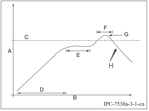
Manner 1: SMT process (Recommended oven temperature curve of reflow soldering)
Set oven temperatures according to the following curve.
-
A: Temperature axis
-
B: Time axis
-
C: Liquidus temperature: 217 to 220°C
-
D: Ramp-up slope: 1 to 3°C/s
-
E: Duration of constant temperature: 60 to 120s; the range of constant temperature: 150 to 200°C
-
F: Duration above the liquidus: 50 to 70s
-
G: Peak temperature: 235 to 245°C
-
H: Ramp-down slope: 1 to 4°C/s
The above curve is just an example of the solder paste SAC305. For more details about other solder pastes, please refer to Recommended oven temperature curve in the solder paste specifications.
Manner 2: Wave soldering process (Oven temperature curve of wave soldering)
Set oven temperatures according to the following temperature curve of wave soldering. The peak temperature is 260°C±5°C.
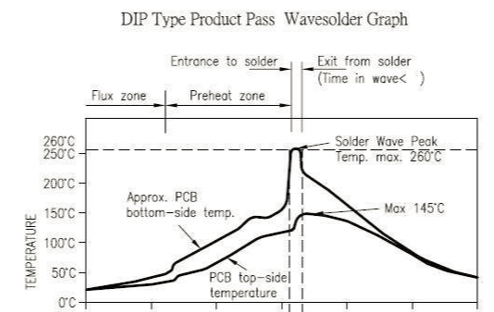
| Suggestions on oven temperature curve of wave soldering | Suggestions on manual soldering temperature | ||
|---|---|---|---|
| Preheat temperature | 80 to 130 °C | Soldering temperature | 360±20°C |
| Preheat time | 75 to 100s | Soldering time | <3s/point |
| Peak contact time | 3 to 5s | NA | NA |
| Temperature of tin cylinder | 260±5°C | NA | NA |
| Ramp-up slope | ≤2°C/s | NA | NA |
| Ramp-down slope | ≤6°C/s | NA | NA |
Storage conditions
MOQ and packaging information
| Product model | MOQ (pcs) | Packing method | Modules per reel | Reels per carton |
|---|---|---|---|---|
| TS24-U | 4400 | Tape reel | 1100 | 4 |
Is this page helpful?
YesFeedbackIs this page helpful?
YesFeedback


