VWBK1 Module Datasheet
VWBK1 is a single-chip Wi-Fi module that supports online voice interaction and IoT applications. Offline and online hybrid interaction solutions can be customized on your terms. In addition, the module supports audio transmission over Bluetooth, helping you develop and empower the entry to voice control of smart speakers and smart home appliances.
Features
- Built-in Wi-Fi MCU, Bluetooth MCU, and CEVA digital signal processor (DSP) kernels.
- Wi-Fi MCU: The maximum clock rate is 240 MHz.
- Bluetooth MCU: The maximum clock rate is 120 MHz.
- DSP: Handle voice interrupts. The maximum clock rate is 320 MHz.
- Operating voltage: 3.3V to 4.2V. And 3.3V/1A power supply is recommended.
- Peripheral interfaces: 12 GPIO interfaces (multiplexing), 2 UART interfaces, 2 ADC interfaces, 8 PWM interfaces (multiplexing), and 1 I2C interface.
- Sampling rate: 16K/16 bit.
- Voice input: With 4 channels of audio ADC built in, the module can be connected to 4 channels of analog microphones.
- Voice output: With 2 channels of stereo output, the module can be connected to an external power amplifier to drive high-power speakers.
- Recommended wake-up distance: no more than 5 meters.
- Recommended operating noise floor: no more than 60 dBc/Hz.
- Wi-Fi connectivity
- Channels 1 to 14 at 2.4 GHz.
- IEEE 802.11 b/g/n20.
- The maximum output power is +16 dBm for 802.11b transmission.
- The onboard PCB antenna or IPEX antenna has a gain of 0.66 dBi.
- Bluetooth connectivity
- Complete Bluetooth v5.0 standard, including Bluetooth Classic (BR/EDR) and Bluetooth Low Energy (LE).
- The output power is up to +3 dBm.
- The Bluetooth LE receiving sensitivity is –88 dBm.
Applications
- Smart speaker
- Voice assistant
- Switch panel
- Light
- Home appliance
- Toy
Module interfaces
Module picture, dimensions, and footprint
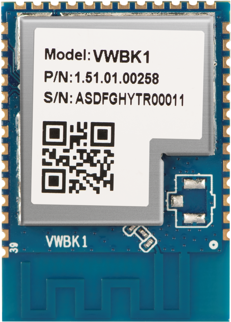
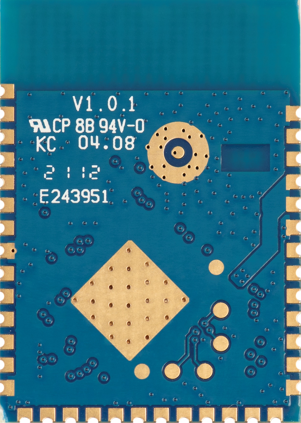
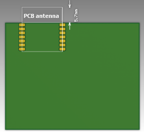
The actual VWBK1 module has an onboard antenna, and its front is a shield cover. Its picture is as follows:
-
Actual picture:
-
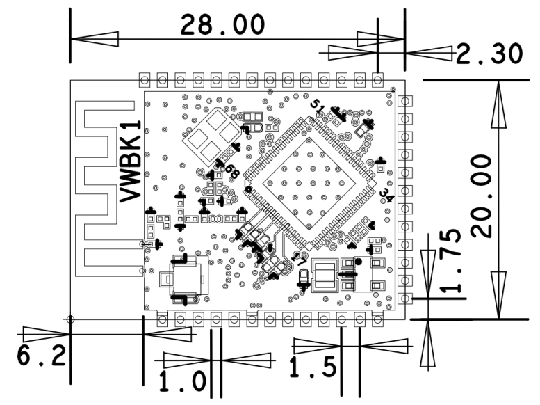
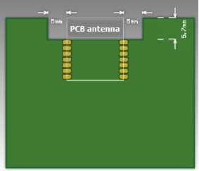
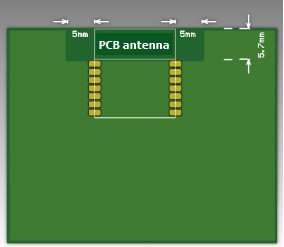
VWBK1 has pins on three sides and an on-board antenna on the other side. There are a total of 39 pins on the three sides, with a 1.5 mm pin spacing. The dimensions of the module are 20 mm (W) × 28 mm (L) × 3.6 mm (H). For more information, see the following diagram. Unit: mm.
Pin definition
The VWBK1 module needs an external microphone, power amplifier, and speaker to complete voice interaction. Its firmware buttons and status indicators shall meet specific requirements. Tuya recommends the following default peripherals required by the voice module.
-
Microphone (required): Two external microphones must be connected at a distance of 35 mm to 80 mm from each other. For more information about specifications, please contact your Tuya account manager.
-
Power amplifier (required): For more information about specifications, please contact your Tuya account manager.
-
Speaker (required): For more information about specifications and structural design, please contact your Tuya account manager.
-
Voice status indicator (required): Three lighting effects are available for the Amazon voice system, including three-color single light, ring light, and line light.
-
Button (required): Several buttons are available, including mute, pause, volume up, and volume down.
The module provides a bunch of interfaces for power supply, indicator, audio, and many other functions. The schematic diagram is as follows:
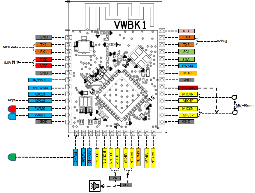
The module has a total of 39 pins. The following table lists the specific pins and their functional descriptions.
| Pin No. | Feature | Type | Functional description |
|---|---|---|---|
| 2 | TX1 | I/O | TX1 of the serial port, used for communication between the module and MCU. |
| 3 | RX1 | I/O | RX1 of the serial port, used for communication between the module and MCU. |
| 4 and 5 | VCC | P | Power input. |
| 1, 6, 13, 26, and 32 | GND | P | Ground. |
| 7 | DN/PWM3 | I/O | The DN interface of USB. It can also be used as PWM3. It is reserved for the cool light. |
| 8 | DP/PWM4 | I/O | The DP interface of USB. It can also be used as PWM4. It is reserved for the warm light. |
| 9 | ADC13 | AI/IO | The ADC13 interface, reserved for peripherals. It can be used as GPIO when the GPIO interface is insufficient. |
| 10 | ADC12 | AI/IO | The ADC12 interface. It can be connected to volume up, volume down, phone, and other buttons. |
| 11 | PWM9 | I/O | The PWM9 dimming interface. By default, it is the voice status indicator in red. |
| 12 | PWM8 | I/O | The PWM8 dimming interface. By default, it is the voice status indicator in green. |
| 14 | PWM7 | I/O | The PWM7 dimming interface. By default, it is the voice status indicator in blue. |
| 15 | PWM6 | I/O | Reserved. It is used to drive the green light and is reserved for the infrared TX. |
| 16 | PWM10 | I/O | Reserved. It is used to drive the red light and is reserved for the infrared RX. |
| 17 | ROUT-P | AO | Positive output for the right channel. It is reserved for an external power amplifier to drive the speaker. |
| 18 | ROUT-N | AO | Negative output for the right channel. It is reserved for an external power amplifier to drive the speaker. |
| 19 | LOUT-N | AO | Negative output for the left channel. It is reserved for an external power amplifier to drive the speaker. |
| 20 | LOUT-P | AO | Positive output for the left channel. It is reserved for an external power amplifier to drive the speaker. |
| 21 | MIC1P | AI | The positive pole of microphone 1, used as the input interface of AEC. |
| 22 | MIC1N | AI | The negative pole of microphone 1, used as the input interface of AEC. |
| 23 | GPIO24 | I/O | Used for power amplifier enable control, marked as SPK-EN. |
| 24 | MIC2P | AI | The positive pole of microphone 2, used as the input interface of AEC. |
| 25 | MIC2N | AI | The negative pole of microphone 2, used as the input interface of AEC. |
| 27 | MIC3P | AI | The positive pole of microphone 3, connected to a microphone. |
| 28 | MIC3N | AI | The negative pole of microphone 3, connected to a microphone. |
| 29 | MIC4P | AI | The positive pole of microphone 4, connected to a microphone. |
| 30 | MIC4N | AI | The negative pole of microphone 4, connected to a microphone. |
| 31 | MICBIAS | P | The power output of the microphone. It is used to power the external microphone. |
| 33 | GPIO2 | I/O | The input signal, used to detect the mute state of a microphone. |
| 34 | PWM0 | I/O | PWM0 driver, used to drive the blue light. |
| 35 | SDA | I/O | The I2C data interface, with a pull-up resistor required. It can drive ring lights and other I2C sensors. |
| 36 | SCL | I/O | The I2C clock interface, with a pull-up resistor required. It can drive ring lights and other I2C sensors. |
| 37 | TX3 | I/O | The UART3 TX interface for debugging. |
| 38 | RX3 | I/O | The UART3 RX interface for debugging. |
| 39 | RST | I | The module reset pin. |
I/O is a general-purpose input and output pin, P is a power supply and ground pin, AI is an analog input pin, and AO is an analog output pin.
Electrical parameters
Absolute electrical parameters
| Parameter | Description | Min value | Max value | Unit |
|---|---|---|---|---|
| Ts | Storage temperature | -55 | 125 | °C |
| VCC | Supply voltage | 3.3V | 4.2 | V |
| Electrostatic discharge voltage (human body model) | TAMB -25°C | N/A | ±2000 | kV |
| Electrostatic discharge voltage (machine model) | TAMB -25°C | N/A | N/A | kV |
Operating voltage: 3.3V to 4.2V. And 3.3V power supply is recommended.
Operating conditions
| Parameter | Description | Min value | Typical value | Max value | Unit |
|---|---|---|---|---|---|
| Ta | Operating temperature | -20 | 25 | 85 | °C |
| VCC | Operating voltage | 3.3 | 3.3 | 4.2 | V |
| Vil | I/O low-level input | -0.3 | N/A | 1.32 | V |
| Vih | I/O high-level input | 2.06 | N/A | 3.6 | V |
| Vol | I/O low-level output | -0.3 | N/A | 0.4 | V |
| Voh | I/O high-level output | 2.9 | N/A | 3.6 | V |
| Imax | I/O drive current | -35 | N/A | 35 | mA |
Wi-Fi transmit and receive power consumption
| Working status | Mode | Rate | Transmit/Receive power | Average value | Peak (Typical) value | Unit |
|---|---|---|---|---|---|---|
| Transmit | 11b | 11 Mbit/s | +16 dBm | 279 | 313 | mA |
| Transmit | 11g | 54 Mbit/s | +14 dBm | 280 | 309 | mA |
| Transmit | 11n | MCS7 | +13 dBm | 274 | 304 | mA |
| Receive | 11b | 11 Mbit/s | Continuous reception | 184 | 187 | mA |
| Receive | 11g | 54 Mbit/s | Continuous reception | 184 | 187 | mA |
| Receive | 11n | MCS7 | Continuous reception | 184 | 187 | mA |
VBAT is 3.3V.
Power consumption in working mode
| Working mode | Working state, Ta=25°C, VCC=3.3V, not connected to PA power amplifier and speaker |
Average value | Max value | Unit |
|---|---|---|---|---|
| Pairing in EZ mode | The module is being paired in EZ mode. | 187 | 568 | mA |
| Idle network connection | The module is connected to the internet. | 165 | 341 | mA |
| Voice control | The module is connected to the internet and woken up by voice. | 240 | 564 | mA |
RF features
Basic RF features
| Parameter | Description |
|---|---|
| Operating frequency | 2.400 to 2.484 GHz |
| Wi-Fi standard | IEEE 802.11b/g/n (channels 1–14) |
| Data transmission rate |
|
| Antenna type | Onboard PCB antenna with a gain of 0.66 dBi. |
Transmitter (TX) performance
TX continuous transmission performance
| Parameter | Min value | Typical value | Max value | Unit |
|---|---|---|---|---|
| RF average output power, 802.11b CCK mode, 11M | - | 16 | - | dBm |
| RF average output power, 802.11g OFDM mode, 54M | - | 14 | - | dBm |
| RF average output power, 802.11n OFDM mode, MCS7 | - | 13 | - | dBm |
| RF average output power, Bluetooth LE/BR/EDR 1M | - | 3 | - | dBm |
| EVM@802.11b CCK 11 Mbit/s mode, 16 dBm | - | -23 | - | dB |
| EVM@802.11g OFDM 54 Mbit/s mode, 13.5 dBm | - | -27 | - | dB |
| EVM@802.11n OFDM MCS7 mode, 12 dBm | - | -28 | - | dB |
| Frequency error | -20 | - | 20 | ppm |
Receiver (RX) performance
RX sensitivity
| Parameter | Min value | Typical value | Max value | Unit |
|---|---|---|---|---|
| PER < 8%, RX sensitivity, 802.11b DSSS mode, 11M | - | -87 | - | dBm |
| PER < 10%, RX sensitivity, 802.11g OFDM mode, 54M | - | -71 | - | dBm |
| PER < 10%, RX sensitivity, 802.11n OFDM mode, MCS7 | - | -68 | - | dBm |
| PER < 30%, RX sensitivity, Bluetooth LE, 1M | - | -88 | - | dBm |
Antenna information
Antenna type
The PCB antenna used by VWBK1 is a MIFA onboard antenna that supports a 2.4 GHz Wi-Fi frequency band.
Antenna interference reduction
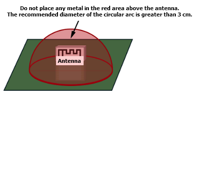
When a PCB antenna is used on a Wi-Fi module, we recommend that the module antenna is at least 15 mm away from other metal components. This can optimize the Wi-Fi performance.
Make sure that the enclosure surrounding the antenna is not traced or filled with copper. Otherwise, the RF performance might be degraded.
Production instructions
Package the module with the SMT if Tuya’s module is designed to be SMT-packaged. After being unpacked, the module must be soldered within 24 hours. Otherwise, it needs to be put into a drying cupboard with a relative humidity level no greater than 10%, or pack the module in vacuum again. Then, record the packing time and duration of exposure. The total exposure time cannot exceed 168 hours.
-
Instruments or devices required for the SMT process:
- Surface mount system
- SPI
- Reflow soldering
- Thermal profiler
- Automated optical inspection (AOI) equipment
-
Instruments or devices required for the baking process:
- Cabinet oven
- Anti-electrostatic and heat-resistant trays
- Anti-electrostatic and heat-resistant gloves
-
A delivered module must meet the following storage requirements:
-
The moisture-proof bag must be placed in an environment where the temperature is below 40°C and the relative humidity is lower than 90%.
-
The shelf life of a dry-packaged product is 12 months from the date when the product is packaged and sealed.
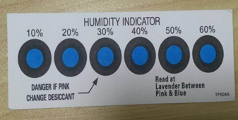
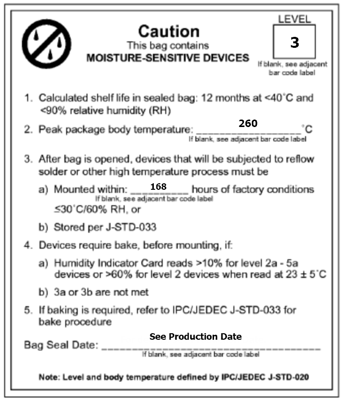
A humidity indication card (HIC) is put in the sealed package.
-
-
The module needs to be baked in the following cases:
- The vacuum packaging bag is damaged before unpacking.
- After unpacking, no HIC is found in the packaging bag.
- After unpacking, the HIC indicates a humidity level of 10% or higher (the circle turns pink on the HIC).
- The total exposure time has lasted for over 168 hours since unpacking.
- More than 12 months have passed since the first sealing of the bag.
-
The baking parameter settings are described below:
- Baking temperature: 60°C for reel packaging with relative humidity ≤ 5%. And 125°C for tray packaging with relative humidity ≤ 5% (use the heat-resistant tray, rather than plastic containers).
- Baking time: 48 hours for reel packaging and 12 hours for tray packaging.
- Temperature for triggering an alert: 65°C for reel packaging and 135°C for tray packaging.
- Production can begin after a module has cooled below 36°C under natural conditions.
- If a module remains unused for over 168 hours after being baked, it needs to be baked again.
- If a batch of modules is not baked after exposure for more than 168 hours, do not use reflow soldering to solder them. Because these modules are level-3 moisture-sensitive devices, they are very likely to get damp when exposed beyond the allowable time. In this case, if they are soldered at high temperatures, device failure or poor soldering performance might occur.
In the whole production process, take electrostatic discharge (ESD) protective measures. To guarantee the pass rate, we recommend that you use the SPI and AOI to monitor the quality of solder paste printing and mounting.
-
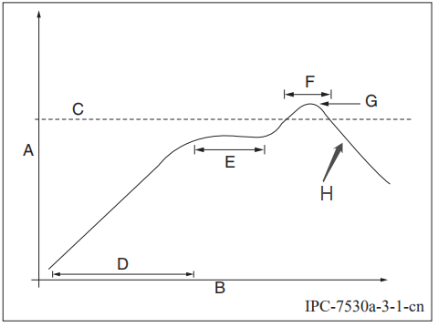
Recommended oven temperature curve
Perform the SMT process according to the following temperature curve of reflow soldering. The peak temperature is 245°C.
-
A: temperature axis
-
B: time axis
-
C: alloy liquidus temperature from 217°C to 220°C
-
D: ramp-up slope from 1°C/s to 3°C/s
-
E: keep a constant temperature from 150°C to 200°C for a time period of 60s to 120s
-
F: temperature above liquidus temperature for 50s to 70s
-
G: peak temperature from 235°C to 245°C
-
H: ramp-down slope from 1°C/s to 4°C/s
The curve above is based on solder paste SAC305. For more information about other solder pastes, see the recommended oven temperature curve in the specified solder paste specifications.
-
-
Storage conditions
Values are in millimeters (mm).
Is this page helpful?
YesFeedbackIs this page helpful?
YesFeedback


