BCNU Module Datasheet
This topic describes Tuya’s proprietary BCNU Bluetooth low energy (LE) module. It consists of a highly integrated Bluetooth chip, TLSR8250, and a few peripheral circuits. It has built-in Bluetooth protocol stacks and a rich set of library functions.
Overview
The BCNU module is built around a 32-bit microcontroller unit (MCU) with 4 Mbits of flash and 48 KB of SRAM. The embedded 2.4 GHz transceiver supports Bluetooth 5.
Features
- Built-in low-power 32-bit MCU that also acts as an application processor
- Clock rate of 48 MHz
- Operating voltage range: 3.0V to 3.6V
- Peripherals: 15 general-purpose input/output (GPIO) pins, 1 universal asynchronous receiver/transmitter (UART), and 2 analog-to-digital converter (ADC) pins
- Bluetooth LE radio frequency (RF) features
- Compatible with Bluetooth LE 4.2/5.0
- Transmitter (TX) power: +10 dBm
- Receiver (RX) sensitivity: -94.5 dBm@Bluetooth LE 1 Mbit/s
- Embedded hardware Advanced Encryption Standard (AES) encryption
- Onboard PCB antenna with a gain of 1.1 dBi
- Operating temperature range: -40°C to +85°C
Scope of applications
- Smart building
- Smart home and electrical appliance
- Smart socket and light
- Industrial wireless control
- Baby monitor
- Smart bus
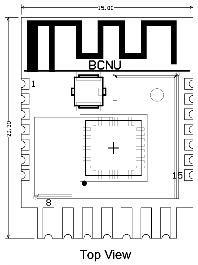
Module interfaces
Dimensions and footprint
BCNU has three rows of pins with a 1.4±0.1mm pin spacing. The BCNU dimensions are 20.3±0.35 mm (L) × 15.8±0.35 mm (W) × 3.0±0.15 mm (H).
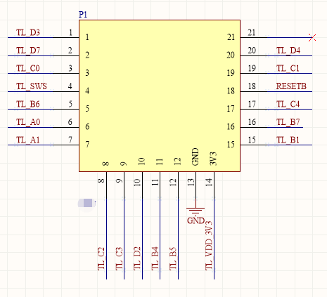
Pinout
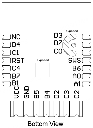
| Pin No. | Symbol | I/O type | Description |
|---|---|---|---|
| 1 | D3 | I/O | GPIO pin, corresponding to D3 (Pin 32) on the IC. |
| 2 | D7 | I/O | GPIO pin, corresponding to D7 (Pin 2) on the IC. |
| 3 | C0 | I/O | GPIO pin, corresponding to C0 (Pin 20) on the IC. |
| 4 | SWS | I/O | Used for firmware flashing, corresponding to SWS (Pin 5) on the IC. |
| 5 | B6 | I | ADC pin, corresponding to B6 (Pin 16) on the IC. |
| 6 | A0 | I/O | GPIO pin, corresponding to A0 (Pin 3) on the IC. |
| 7 | A1 | I/O | GPIO pin, corresponding to A1 (Pin 4) on the IC. |
| 8 | C2 | I/O | Support hardware PWM, corresponding to C2 (Pin 22) on the IC. |
| 9 | C3 | I/O | Support hardware PWM, corresponding to C3 (Pin 23) on the IC. |
| 10 | D2 | I/O | Support hardware PWM, corresponding to D2 (Pin 31) on the IC. |
| 11 | B4 | I/O | Support hardware PWM, corresponding to B4 (Pin 14) on the IC. |
| 12 | B5 | I/O | Support hardware PWM, corresponding to B5 (Pin 15) on the IC. |
| 13 | GND | P | Ground pin. |
| 14 | VCC | P | Power supply pin (3.3V). |
| 15 | B1 | I/O | Uart_TXD, corresponding to B1 (Pin 6) on the IC. |
| 16 | B7 | I/O | Uart_RXD, corresponding to B7 (Pin 17) on the IC. |
| 17 | C4 | I/O | ADC pin, corresponding to C4 (Pin 24) on the IC. |
| 18 | RST | I/O | Reset pin. Active low. |
| 19 | C1 | I/O | GPIO pin, corresponding to C1 (Pin 21) on the IC. |
| 20 | D4 | I/O | GPIO pin, corresponding to D4 (Pin 1) on the IC. |
| 21 | NC | I/O | Not connected. |
P indicates the power pin, and I/O indicates the input and output pin.
Electrical parameters
Absolute electrical parameters
| Parameter | Description | Minimum value | Maximum value | Unit |
|---|---|---|---|---|
| Ts | Storage temperature | -65 | 150 | °C |
| VCC | Supply voltage | -0.3 | 3.9 | V |
| Electrostatic discharge voltage (human body model) | TAMB-25°C | - | 2 | kV |
| Electrostatic discharge voltage (machine model) | TAMB-25°C | - | 0.5 | kV |
Operating conditions
| Parameter | Description | Minimum value | Typical value | Maximum value | Unit |
|---|---|---|---|---|---|
| Ta | Operating temperature | -40 | - | 85 | °C |
| VCC | Operating voltage | 3.0 | 3.3 | 3.6 | V |
| VIL | I/O low-level input | VSS | - | VCC × 0.3 | V |
| VIH | I/O high-level input | VCC × 0.7 | - | VCC | V |
| VOL | I/O low-level output | VSS | - | VCC × 0.1 | V |
| VOH | I/O high-level output | VCC × 0.9 | - | VCC | V |
Power consumption in working mode
| Symbol | Condition | Max (Typical) value | Unit |
|---|---|---|---|
| Itx | Continuous transmission, with an output power of 11.5 dBm | 22.6 | mA |
| Irx | Continuous reception | 6.5 | mA |
| IDC | Average value when connected over Bluetooth mesh | 6.59 | mA |
| IDC | Peak value when connected over Bluetooth mesh | 24.9 | mA |
| I deepsleep1 | Deep sleep mode (16 KB RAM reserved) | 1.2 | μA |
| I deepsleep2 | Deep sleep mode (RAM not reserved) | 0.4 | μA |
RF parameters
Basic RF features
| Parameter | Description |
|---|---|
| Operating frequency | 2.4 GHz ISM band |
| Wireless standard | Bluetooth LE 4.2/5.0 |
| Data transmission rate | 1 Mbit/s |
| Antenna type | Onboard PCB antenna |
RF output power
| Parameter | Minimum value | Typical value | Maximum value | Unit |
|---|---|---|---|---|
| RF average output power | -21 | 10 | 11.5 | dBm |
| Bandwidth of 20 dB modulation signal (1 Mbit/s) | - | 2500 | - | kHz |
RF receiver (RX) sensitivity
| Parameter | Minimum value | Typical value | Maximum value | Unit |
|---|---|---|---|---|
| RX sensitivity 1 Mbit/s | - | -94.5 | - | dBm |
| Frequency offset error 1 Mbit/s | -250 | - | +300 | kHz |
| Co-channel interference suppression | - | - | -10 | dB |
Power-up sequence of the module
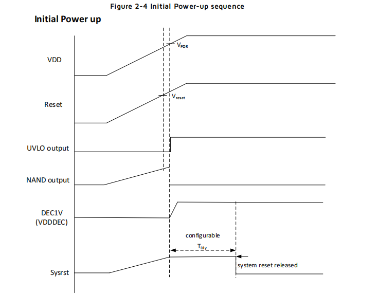
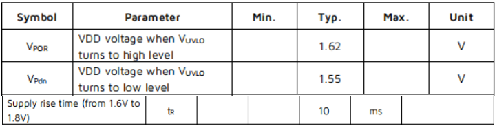
The TLSR8250 chip has requirements for the power-up sequence. During the power-up process, the system begins to start after the RST pin reaches 1.62V. At this time, the VDD pin needs to reach above 1.8V within 10 ms. The RST pin has an RC link. When the RST pin reaches 1.62V, the VDD pin of the bare module has far exceeded 1.8V.
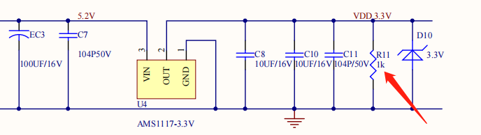
If the power driver connected to a module with a TLSR8250 chip is charged and discharged by a large capacitor, and the module voltage is not fully discharged below 0.6V, the module might crash when restarted. The VDD_3.3V power supply pin of the module needs to be connected to a 1K dummy load to speed up discharge. The figure below shows part of the power drive link for your reference.
Antenna information
Antenna type
Onboard PCB antenna with a gain of 1.1 dBi.
Antenna interference reduction
The distance between the antenna and other metal components should be at least 15 mm to provide the best radio performance. If metal materials wrap the surroundings of the antenna, the wireless signal will be greatly attenuated, thereby deteriorating the RF performance. Allow enough space to support the RF layout when designing your product.
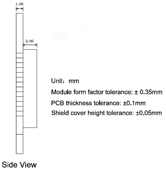
Footprint and production instructions
Mechanical dimensions
The PCB dimensions are 20.3±0.35 mm (L) × 15.8±0.35 mm (W) × 1.0±0.1 mm (H).
Side view
Pinout
Surface-mount technology (SMT) package

The area indicated as keep-out in the diagram above does not require tinning and should not have any traces routed through it.
Production instructions
-
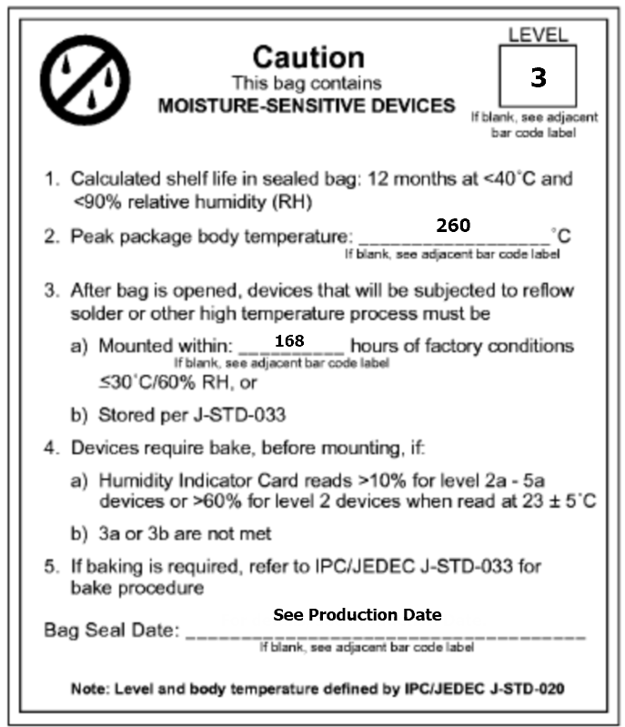
For the modules that can be packaged with the surface-mount technology (SMT) or in in-line form, you can select either of them according to the PCB design solutions of customers. If a PCB is designed to be SMT-packaged, package the module with the SMT. If a PCB is designed to use an in-line package, use wave soldering. Complete soldering within 24 hours after the module is unpacked. Otherwise, we recommend that you place the module in a drying cupboard with a relative humidity level below 10%, or pack the module in a vacuum again. Then, record the packing time and duration of exposure. The total exposure time cannot exceed 168 hours.
- Instruments or devices required for the SMT process:
- Surface mount system
- SPI
- Reflow soldering machine
- Thermal profiler
- Automated optical inspection (AOI) equipment
- Instruments or devices required for the wave soldering process:
- Wave soldering device
- Wave soldering fixture
- Constant-temperature soldering iron
- Tin bar, tin wire, and flux
- Thermal profiler
- Instruments or devices required for the baking process:
- Cabinet oven
- Electrostatic discharge (ESD) protection and heat-resistant trays
- ESD protection and heat-resistant gloves
- Instruments or devices required for the SMT process:
-
A delivered module must meet the following storage requirements:
-
The moisture-proof bag must be placed in an environment where the temperature is below 40°C and the relative humidity is lower than 90%.
-
The shelf life of a dry-packaged product is 12 months from the date when the product is packaged and sealed.
-
A humidity indication card (HIC) is put in the sealed package.
-
-
The module needs to be baked in the following cases:
- The vacuum packaging bag is damaged before unpacking.
- After unpacking, no HIC is found in the packaging bag.
- After unpacking, the HIC indicates a humidity level of 10% or higher. In this case, the circle turns pink on the HIC.
- The total exposure time has lasted for over 168 hours since unpacking.
- More than 12 months have passed since the first sealing of the bag.
-
The baking parameter settings are described below:
- Baking temperature: 40°C for reel packaging with relative humidity ≤ 5%. And 125°C for tray packaging with relative humidity ≤ 5% (use a heat-resistant tray, rather than a plastic container).
- Baking time: 168 hours for reel packaging and 12 hours for tray packaging.
- Temperature for triggering an alert: 50°C for reel packaging and 135°C for tray packaging.
- Production can begin after a module has cooled down to below 36°C under natural conditions.
- If a module remains unused for over 168 hours after being baked, it needs to be baked again.
- If a batch of modules is not baked after exposure for more than 168 hours, do not use wave soldering to solder them. Because these modules are level-3 moisture-sensitive devices, they are very likely to get damp when exposed beyond the allowable time. In this case, if they are soldered at high temperatures, device failure or poor soldering performance might occur.
-
In the whole production process, take electrostatic discharge (ESD) protective measures.
-
To guarantee the pass rate, we recommend that you use the SPI and AOI to monitor the quality of solder paste printing and mounting.
Recommended oven temperature curve
Select a proper soldering technique according to the process. For more information, refer to the recommended oven temperature curve of either reflow soldering or wave soldering. The set temperatures might deviate from the actual temperature measurements. All temperatures shown in this module datasheet are obtained through actual measurements.
Technique 1: SMT process (recommended oven temperature curve of reflow soldering)
Set the oven temperatures according to the following curve.
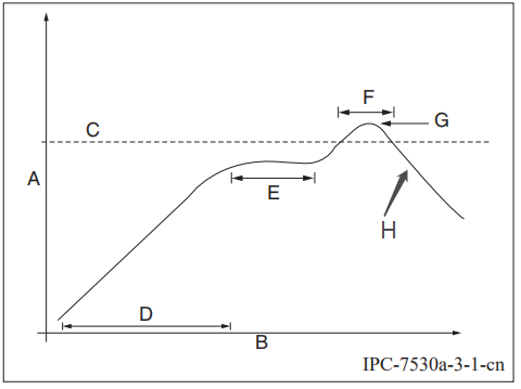
-
A: temperature axis
-
B: time axis
-
C: alloy liquidus temperature from 217°C to 220°C
-
D: ramp-up slope from 1°C/s to 3°C/s
-
E: keep a constant temperature from 150°C to 200°C for a time period of 60s to 120s
-
F: temperature above liquidus temperature for 50s to 70s
-
G: peak temperature from 235°C to 245°C
-
H: ramp-down slope from 1°C/s to 4°C/s
The curve above is based on solder paste SAC305. For more information about other solder pastes, see the recommended oven temperature curve in the specified solder paste specifications.
Technique 2: Wave soldering process (oven temperature curve of wave soldering)
Set the oven temperatures according to the following temperature curve of wave soldering. The peak temperature is 260°C±5°C.
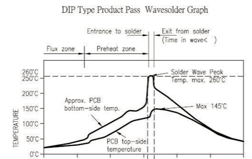
| Suggestions on wave soldering | Suggestions on manual repair soldering | ||
|---|---|---|---|
| Preheat temperature | 80°C to 130°C | Soldering temperature | 360°C ± 20°C |
| Preheat duration | 75s to 100s | Soldering duration | Less than 3s/point |
| Contact duration at the peak | 3s to 5s | N/A | N/A |
| Solder tank temperature | 260°C ± 5°C | N/A | N/A |
| Ramp-up slope | ≤ 2°C/s | N/A | N/A |
| Ramp-down slope | ≤ 6°C/s | N/A | N/A |
Storage conditions
MOQ and packaging information
| Product model | MOQ (pcs) | Shipping packaging | Modules per reel | Reels per carton |
|---|---|---|---|---|
| BCNU | 4,400 | Tape and reel | 1,100 | 4 |
Is this page helpful?
YesFeedbackIs this page helpful?
YesFeedback


