

BT2S Module Datasheet
BT2S is an embedded low-power Bluetooth module that Tuya has developed. It consists of a highly integrated Bluetooth chip (TLSR8250F512ET32) and several peripheral components, with an embedded Bluetooth network protocol stack and rich library functions.
Overview
BT2S contains a low-power 32-bit MCU, Bluetooth LE 5.0 component, 2.4 GHz radio component, 4-MB flash memory, and 48-KB SRAM.
Features
- Embedded low-power 32-bit MCU, which can also function as an application processor
- Clock rate: 48 MHz
- Working voltage: 3.0 V to 3.6 V
- Peripherals: 5×GPIO, 1×UART, 1×ADC
- Bluetooth LE RF features
- Compatible with Bluetooth LE 4.2/5.0
- Up to 2 Mbit/s RF data rate
- TX power: +10 dBm
- RX sensitivity: -94 dBm at Bluetooth LE 1 Mbit/s
- Embedded advanced encryption standard (AES) hardware encryption
- Onboard PCB antenna with 0.89 dBi gain
- Working temperature: -20°C to +85°C
Applications
- Smart LED lights
- Smart households
- Smart low-power sensors
Module interfaces
Dimensions and footprint
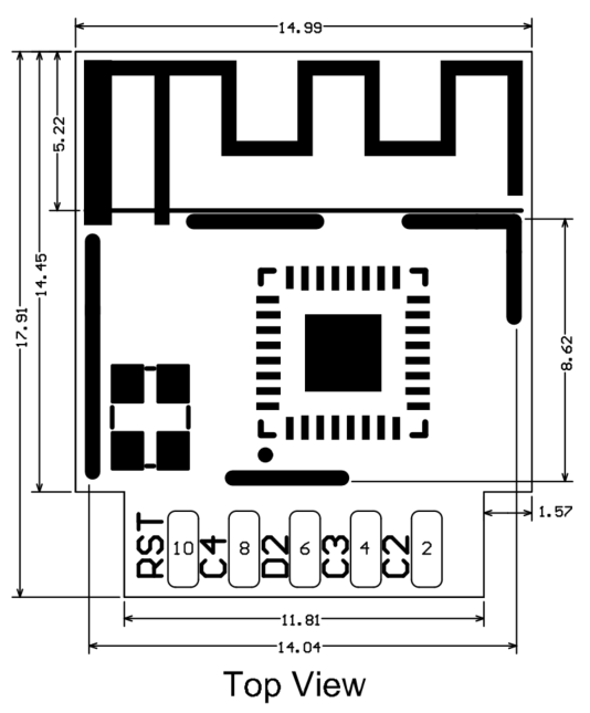
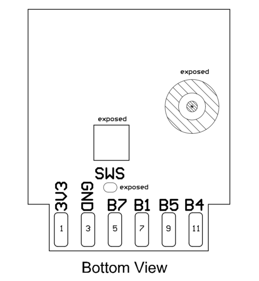
BT2S has two lines of pins with a 2 mm pin spacing.
The BT2S dimensions are 15 ± 0.35 mm (W) × 18 ± 0.35 mm (L) × 2.9 ± 0.15 mm (H). The PCB thickness is 0.8 ± 0.1 mm. The BT2S pins are shown below:
Interface pin definition
| Pin No. | Symbol | I/O type | Function |
|---|---|---|---|
| 1 | 3V3 | P | Power supply pin |
| 2 | C2 | I/O | Common I/O, which can be used as a PWM output of the LED drive and is connected to pin PC2 on the IC |
| 3 | GND | P | Power supply reference ground pin |
| 4 | C3 | I/O | Common I/O, which can be used as a PWM output of the LED drive and is connected to pin PC3 on the IC |
| 5 | B7 | I/O | UART_RX and is connected to pin PB7 on the IC |
| 6 | D2 | I/O | Common I/O, which can be used as a PWM output of the LED drive and is connected to pin PD2 on the IC |
| 7 | B1 | I/O | UART_TX and is connected to pin PB1 on the IC |
| 8 | C4 | AI | SAR ADC Input, and is connected to pin PC4 on the IC |
| 9 | B5 | I/O | Common I/O, which can be used as a PWM output of the LED drive and is connected to pin PB5 on the IC |
| 10 | RST | 1/O | Reset, and is connected to pin 25 on the IC |
| 11 | B4 | I/O | Common I/O, which can be used as a PWM output of the LED drive and is connected to pin PB4 on the IC |
Note:
Pindicates power supply pins, I/O indicates input/output pins and AI indicates analog input pins.- If you have special requirements on light colour controlled by PWM outputs, contact Tuya business personnel.
Electrical parameters
Absolute electrical parameters
| Parameter | Description | Minimum value | Maximum value | Unit |
|---|---|---|---|---|
| Ts | Storage temperature | -65 | 150 | °C |
| VCC | Power supply voltage | -0.3 | 3.9 | V |
| ESD voltage (human body model) | TAMB-25°C | - | 2 | kV |
| ESD voltage (machine model) | TAMB-25°C | - | 0.5 | kV |
Electrical conditions
| Parameter | Description | Minimum value | Typical value | Maximum value | Unit |
|---|---|---|---|---|---|
| Ta | Working temperature | -20 | - | 85 | °C |
| VCC | Working voltage | 3.0 | 3.3 | 3.6 | V |
| VIL | I/O low-level input | VSS | - | VCC*0.3 | V |
| VIH | I/O high-level input | VCC*0.7 | - | VCC | V |
| VOL | I/O low-level output | VSS | - | VCC*0.1 | V |
| VOH | I/O high-level output | VCC*0.9 | - | VCC | V |
Working current
| Symbol | Condition | Minimum Value (Typical) | Unit |
|---|---|---|---|
| Itx | Constant transmission, 11.5 dBm output power | 23.5 | mA |
| Irx | Constant receiving | 6.5 | mA |
| IDC | Connected to a mesh network (Average) | 6.59 | mA |
| IDC | Connected to a mesh network (Peak) | 24.9 | mA |
| Ideepsleep1 | Deep sleep mode 1 (16 KB RAM is reserved.) | 1.2 | μA |
| Ideepsleep2 | Deep sleep mode 2 (No RAM is reserved.) | 0.4 | μA |
RF features
Basic RF features
| Parameter | Description |
|---|---|
| Frequency band | 2.4 GHz ISM band |
| Wireless standard | Bluetooth LE 4.2/5.0 |
| Data transmission rate | 1 Mbit/s, 2 Mbit/s |
| Antenna type | Onboard PCB antenna |
RF output power
| Parameter | Minimum value | Typical value | Maximum value | Unit |
|---|---|---|---|---|
| Average RF output power | -21 | 10 | 11.5 | dBm |
| 20 dB modulation signal bandwidth (1 Mbit/s) | - | 2500 | - | kHz |
| 20 dB modulation signal bandwidth (2 Mbit/s) | - | 1400 | - | kHz |
RF RX sensitivity
| Parameter | Minimum value | Typical value | Maximum value | Unit |
|---|---|---|---|---|
| RX sensitivity 1 Mbit/s | - | -94 | - | dBm |
| RX sensitivity 2 Mbit/s | - | -91 | - | dBm |
| Frequency offset 1 Mbit/s | -250 | - | +300 | kHz |
| Frequency offset 2 Mbit/s | -300 | - | +200 | kHz |
| Co-channel interference suppression | - | -10 | - | dB |
Power-up sequence of the module
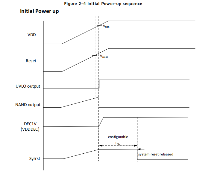
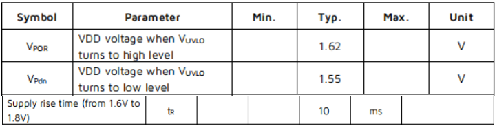
The TLSR8250 chip has specific requirements for the power-up sequence. During the power-up process, the system starts booting after the RST pin reaches 1.62 V. At this point, VDD must rise above 1.8 V within 10 ms. Since the RST pin includes an RC circuit, the VDD voltage of the bare module has already exceeded 1.8 V when RST reaches 1.62 V.
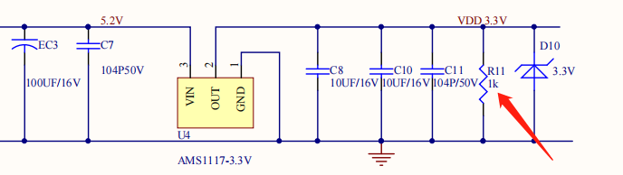
If the power driver connected to a module with a TLSR8250 chip is charged and discharged by a large capacitor, and the module voltage is not fully discharged below 0.6 V, the module might crash when restarted. The VDD_3.3V power supply pin of the module needs to be connected to a 1 kΩ dummy load to accelerate discharge. Refer to the following example power supply driving circuit:
Antenna
Antenna type
BT2S uses an onboard PCB antenna with a gain of 0.89 dBi.
Antenna interference reduction
To ensure optimal RF performance, it is recommended that the antenna be at least 15 mm away from other metal parts. If metal materials are wrapped around the antenna, the wireless signals will be reduced greatly, deteriorating the RF performance. Because BT2S is inserted into the PCB, sufficient space needs to be reserved for the antenna.
Packaging information and production instructions
Mechanical dimensions
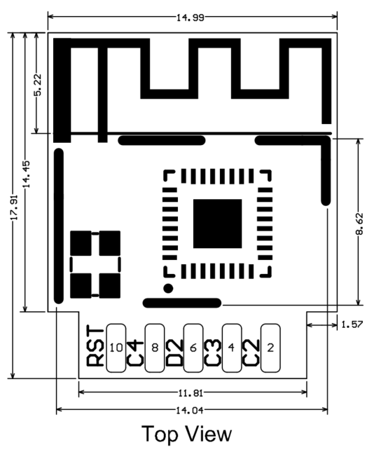
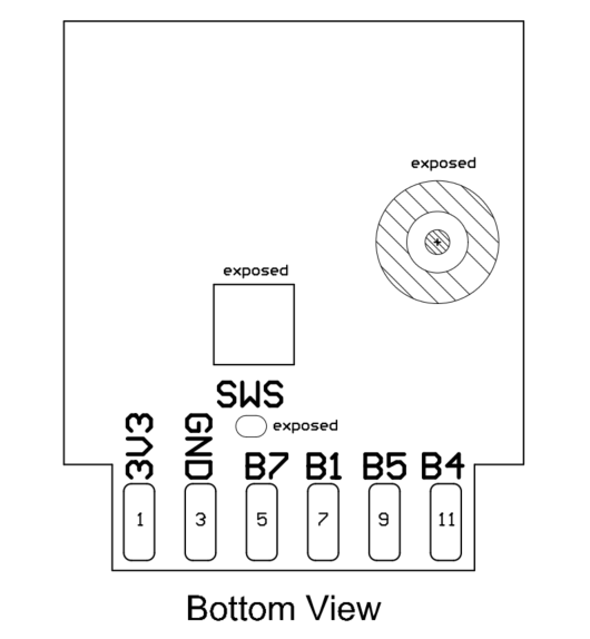
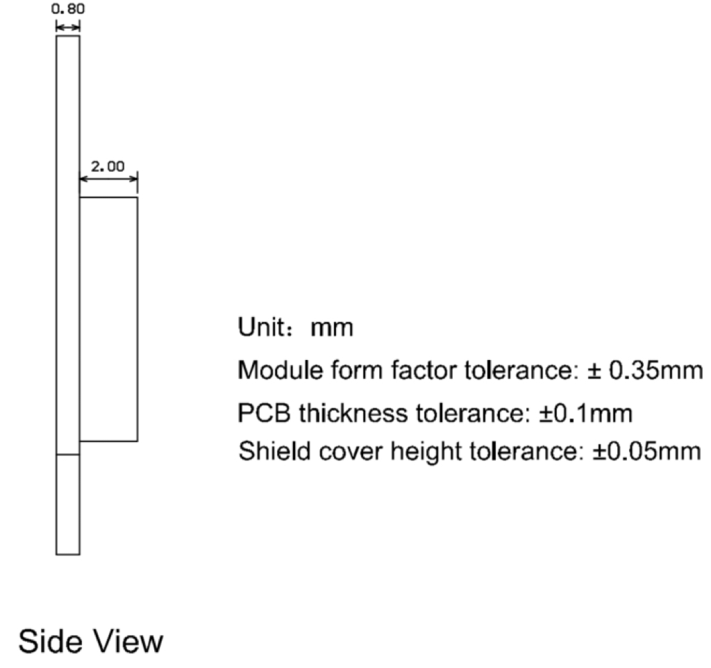
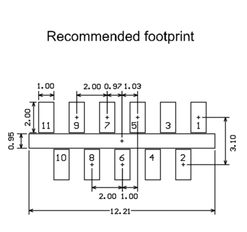
Note:
The default dimensional tolerance is ± 0.35 mm, and the tolerance for some key dimensions is ± 0.1 mm.
Production instructions
-
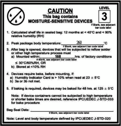
The stamp-hole module must be mounted by the SMT machine. After being unpacked, it must be soldered within 24 hours. Otherwise, it must be put into the drying cupboard where the RH is not greater than 10%, or it needs to be packaged under vacuum again and the exposure time needs to be recorded (the total exposure time cannot exceed 168 hours).
- SMT equipment:
- Mounter
- SPI
- Reflow soldering machine
- Oven temperature tester
- Automated optical inspection (AOI) equipment
- Baking equipment:
- Cabinet oven
- Anti-static heat-resistant pallets
- Anti-static heat-resistant gloves
- SMT equipment:
-
The module needs to be baked in the following cases:
- Vacuum packing bag was found to be damaged before being unpacked.
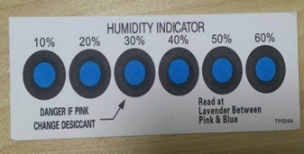
- There is no humidity indicator card (HIC) in the vacuum packing bag.
- After being unpacked, 10% and above circles on the HIC become pink.
- The total exposure time has been more than 168 hours since unpacking.
- More than 12 months have passed since the sealing date of the bag.
-
Baking settings:
- Temperature: 40°C and ≤ 5% RH for reel package and 125°C and ≤5% RH for tray package (please use the heat-resistant tray rather than a plastic container).
- Time: 168 hours for reel package and 12 hours for tray package.
- Alarm temperature: 50°C for reel package and 135°C for tray package.
- Production-ready temperature after natural cooling: < 36°C.
- Re-baking situation: If a module remains unused for over 168 hours after being baked, it needs to be baked again.
- If a batch of modules is not baked within 168 hours, do not use the wave soldering to solder them. Because these modules are Level-3 moisture-sensitive devices, they are very likely to get damp when exposed beyond the allowable time. In this case, if they are soldered at high temperatures, it may result in device failure or poor soldering.
-
In the whole production process, take electrostatic discharge (ESD) protective measures.
-
To guarantee the passing rate, it is recommended that you use the SPI and AOI to monitor the quality of solder paste printing and mounting.
Recommended oven temperature curve
Perform mounting with the SMT based on the following reflow oven temperature curve. The peak temperature is 260 ± 5°C. The reflow temperature curve is as below:
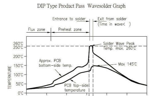
| Suggestions on oven temperature curve of wave soldering | Suggestions on manual soldering temperature | ||
|---|---|---|---|
| Preheat temperature | 80-130°C | Soldering temperature | 360°C±20°C |
| Preheat time | 75-100S | Soldering time | <3s/point |
| Peak contact time | 3-5S | NA | NA |
| Temperature of tin cylinder | 260 ± 5°C | NA | NA |
| Ramp-up slope | ≤2°C/S | NA | NA |
| Ramp-down slope | ≤6°C/S | NA | NA |
Storage conditions
Storage conditions for a delivered module are as follows:
-
The moisture-proof bag must be placed in an environment where the temperature is below 40°C and the relative humidity is lower than 90%.
-
The shelf life of a dry-packaged product is 12 months from the date when the product is packaged and sealed.
-
The package contains a humidity indicator card (HIC).
MOQ and packaging information
| Product model | MOQ (pcs) | Packing method | Number of modules in per reel | Number of reels in per carton |
|---|---|---|---|---|
| BT2S | 4,400 | Tape reel packing | 1,100 | 4 |
Appendix: Statement
FCC Caution: Any changes or modifications not expressly approved by the party responsible for compliance could void the user’s authority to operate this device.
This device complies with Part 15 of the FCC Rules. Operation is subject to the following two conditions: (1) This device may not cause harmful interference, and (2) this device must accept any interference received, including interference that may cause undesired operation.
Note: This device has been tested and found to comply with the limits for a Class B digital device, according to part 15 of the FCC Rules. These limits are designed to provide reasonable protection against harmful interference in a residential installation. This device generates, uses, and can radiate radio frequency energy and, if not installed and used following the instructions, may cause harmful interference to radio communications. However, there is no guarantee that interference will not occur in a particular installation.
If this device does cause harmful interference to radio or television reception, which can be determined by turning the device off and on, the user is encouraged to try to correct the interference by one or more of the following measures:
- Reorient or relocate the receiving antenna.
- Increase the separation between the device and receiver.
- Connect the device into an outlet on a circuit different from that to which the receiver is connected.
- Consult the dealer or an experienced radio/TV technician for help.
Radiation Exposure Statement
This device complies with FCC radiation exposure limits set forth for an uncontrolled rolled environment. This device should be installed and operated with a minimum distance of 20 cm between the radiator and your body.
Important Note
This radio module must not be installed to co-locate and operating simultaneously with other radios in the host system except following FCC multi-transmitter product procedures. Additional testing and device authorization may be required to operate simultaneously with other radios.
The availability of some specific channels and/or operational frequency bands are country dependent and are firmware programmed at the factory to match the intended destination. The firmware setting is not accessible by the end-user.
The host product manufacturer is responsible for compliance with any other FCC rules that apply to the host not covered by the modular transmitter grant of certification. The final host product still requires Part 15 Subpart B compliance testing with the modular transmitter installed.
The end-user manual shall include all required regulatory information/warnings as shown in this manual, including "This product must be installed and operated with a minimum distance of 20 cm between the radiator and user body".
This device has got an FCC ID: 2ANDL-BT2S. The end product must be labeled in a visible area with the following: "Contains Transmitter Module FCC ID: 2ANDL-BT2S".
This device is intended only for OEM integrators under the following conditions:
The antenna must be installed such that 20 cm is maintained between the antenna and users, and the transmitter module may not be co-located with any other transmitter or antenna.
As long as the 2 conditions above are met, further transmitter tests will not be required. However, the OEM integrator is still responsible for testing their end-product for any additional compliance requirements required with this module installed.
Declaration of Conformity European Notice

Hereby, Hangzhou Tuya Information Technology Co., Ltd declares that this module product is in compliance with essential requirements and other relevant provisions of Directive 2014/53/EU,2011/65/EU. A copy of the Declaration of conformity can be found at https://www.tuya.com.

This product must not be disposed of as normal household waste, in accordance with the EU directive for waste electrical and electronic equipment (WEEE-2012/19/EU). Instead, it should be disposed of by returning it to the point of sale, or to a municipal recycling collection point.
The device could be used with a separation distance of 20 cm to the human body.
Is this page helpful?
YesFeedbackIs this page helpful?
YesFeedback