GB600 Module Datasheet
GB600 is a Global Navigation Satellite System (GNSS) module developed by Tuya. It applies to in-vehicle navigation, outdoor positioning, surveying, and mapping products.
Overview
As a single-chip L1 band GNSS module, GB600 consists of a highly integrated, multi-system, low-power, high-performance SoC chip Beken-BK1661, and its peripheral circuits. This module features built-in components such as a surface acoustic wave (SAW) filter, low noise amplifier (LNA), and 26 MHz temperature compensated crystal oscillator (TCXO). It supports multi-mode joint positioning (GPS L1, Beidou B1, Galileo E1, QZSS L1, and GLONASS G1) or single-system independent positioning, thus ensuring fast and accurate positioning results, and providing users with an efficient and convenient positioning experience.
The GB600 module is compact, uses SMT pads, and supports standard pick-and-place and reflow soldering with full automatic integration. It is especially suitable for low-cost, low-power applications.
Features
- Positioning engine:
- 120 simultaneous tracking channels
- Hot start time: < 1.0 second
- Cold start sensitivity: -148 dBm
- Hot start sensitivity: -159 dBm
- Re-capture sensitivity: -159 dBm
- Tracking sensitivity: -165 dBm
- Data update rate: up to 20 Hz
- Support GPS, BDS, Galileo, QZSS, and GLONASS
- RF subsystem adopts a broadband design, and the input signal is centered at about 1575 MHz
- Receive and track GPS’s 1575.42 MHz L1 C/A signal
- Receive and track the BDS satellite navigation system’s 1561.098 MHz B1C/B1I signal
- Receive and track Galileo’s 1575.42 MHz E1 signal
- Receive and track GLONASS’s 1575.42 MHz G1 signal
- Receive and track QZSS’s 1575.42 MHz L1 signal
- GB600 is configured to receive joint positioning signals from five systems by default and can be customized as GPS+BDS, GPS+GLONASS, or a single GNSS system. You can file a service ticket to request the required GNSS firmware.
- Operating voltage range: 2.4V to 3.6V, with the typical voltage of 3.3V
- Internal 26 MHz TCXO
- Protocol and port: Comply with the National Marine Electronics Association (NEMA) protocol. Communicate with the host through the UART.
- Operating temperature range: -40°C to +85°C.
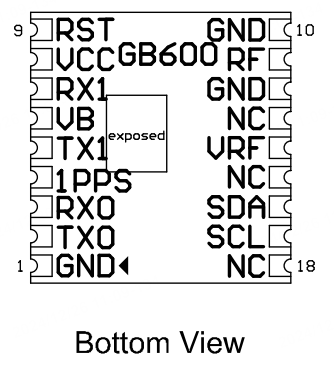
Module interfaces
Pin definition
GB600 is a surface-mounted module with 2 rows of 18 LCC pads and a pin spacing of 1.10 mm.
- GB600 dimensions:
- Width: 9.70 ± 0.35 mm
- Length: 10.10 ± 0.35 mm
- Height: 2.20 ± 0.15 mm
- PCB thickness: 0.8 ± 0.1 mm
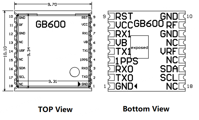
Pin definition
| Pin No. | Symbol | I/O type | Description |
|---|---|---|---|
| 1 | GND | – | The ground pin. |
| 2 | TX0 | O | Main UART, data transmission (TX) of the module’s serial port 0, used for NMEA sentence output, corresponding to GPIO 6 on the chip. |
| 3 | RX0 | I | Main UART, data reception (RX) of the module’s serial port 0, used for PMTK/PQ command input and firmware update, corresponding to GPIO 7 on the chip. |
| 4 | 1PPS | O | Pulse per second. |
| 5 | TX1 | O | Data TX of the module’s serial port 1, corresponding to GPIO 2 on the chip. |
| 6 | VB | PI | The backup power input for the module, ranging from 2.4V to 3.6V, with a typical value of 3.3V. |
| 7 | RX1 | I | Data RX of the module’s serial port 1, corresponding to GPIO 3 on the chip. |
| 8 | VCC | PI | The main power input for the module, ranging from 2.4V to 3.6V, with a typical value of 3.3V. The main power ripple should be less than 50 mVpp, and there should be at least one decoupling capacitor of 2.2 μF or more close to the pin. |
| 9 | RST | I | Reset pin. Active low. |
| 10 | GND | – | The ground pin. |
| 11 | RF | I | GNSS signal input pin (BDS B1, GPS L1, Galileo E1, QZSS L1, and GLONASS G1) |
| 12 | GND | – | The ground pin. |
| 13 | NC | – | Not connected. |
| 14 | VRF | PO | Active antenna feeding output, ranging from 1.7V to 3.1V. The default value is 2.8V. |
| 15 | NC | – | Not connected. |
| 16 | SDA | I/O | I2C_SDA, corresponding to GPIO 9 on the chip. When I2C is used, a pull-up resistor of about 5 KΩ is required to pull up the SDA. |
| 17 | SCL | I/O | I2C_SCL, corresponding to GPIO 8 on the chip. When I2C is used, a pull-up resistor of about 5 KΩ is required to pull up the SCL. |
| 18 | NC | – | Not connected. |
P indicates the power pin, and I/O indicates the input and output pin.
Electrical parameters
Absolute electrical parameters
| Parameter | Description | Min value | Max value | Unit |
|---|---|---|---|---|
| Ts | Storage temperature | -40 | 150 | °C |
| VCC | Supply voltage | -0.3 | 3.6 | V |
| Electrostatic discharge voltage (human body model) | TAMB -25°C | – | TBD | kV |
| Electrostatic discharge voltage (machine model) | TAMB -25°C | – | TBD | kV |
Normal operating conditions
| Parameter | Description | Min value | Typical value | Max value | Unit |
|---|---|---|---|---|---|
| Ta | Operating temperature | -40 | 25 | 85 | °C |
| VCC | Supply voltage | 2.4 | 3.3 | 3.6 | V |
| V_BCKP | Backup voltage | 2.4 | 3.3 | 3.6 | V |
Power consumption in working mode
| Working mode | Parameter | Average value | Peak (Typical) value | Unit |
|---|---|---|---|---|
| Capture | VCC_IN current | 20.5 | 24.5 | mA |
| Tracking | VCC_IN current | 21.5 | 26.3 | mA |
The test is performed on a passive ceramic antenna with firmware R3.2.10.0 Build 8016, placed in a GB600 supporting evaluation kit (EVK), and fed with 3.3V VCC_IN.
Key specifications
| Parameter | Conditions | Metrics | Unit |
|---|---|---|---|
| CN0 calibration | Signal strength of the simulator: -130 dBm (AVG) | 40 ± 2 | dBc |
| Time to first fix (TTFF) in static mode and under open sky conditions | Cold start, hot start, and recapture | 28/1.0/2 | Second |
| Sensitivity | Capture and tracking | -159/-165 | dBm |
| Positioning accuracy | CEP50 in static mode and under open sky conditions | 1.5 | Meter |
| Antenna | Antenna provided by the third party with the characteristic impedance of 50Ω | – | – |
Antenna information
The GB600 module receives signals from the GPS L1 band (1575.42 MHz) and BDS B1 band (1561 MHZ) by default. The RF signal is input through the RF pin, and the characteristic impedance of the RF port must be controlled at 50Ω, with the trace kept as short as possible.
Antenna parameters recommendation
The GB600 module can receive satellite signals by connecting a dedicated active or passive antenna. The antenna performance has a crucial impact on the receiving sensitivity of the entire GNSS system. The following table shows the recommended antenna specifications.
| Passive antenna parameter | Specification | Remarks |
|---|---|---|
| Dimensions | 25 mm × 25 mm × 4 mm | – |
| RX frequency range | 1561 to 1575 MHz | Center frequency: 1561 ± 3 MHz, 1575 ± 3MHz |
| Characteristic impedance | 50Ω | – |
| Bandwidth | 15 MHz minimum | Return loss ≤ -10 dB |
| Frequency temperature coefficient | 0 ± 10 ppm/°C | -40°C to 85°C |
| Polarization | RHCP | Right-handed circular polarization (RHCP) |
| Gain | 1.5 dBi typical | – |
| Axial ratio | 5 dB maximum | – |
| VSWR | 1.5 maximum | – |
| Active antenna parameter | Specification | Remarks |
|---|---|---|
| RX frequency range | GPS L1 band: 1575.42 ± 1.023 MHz BDS B1 band: 1561 ± 2.046 MHz |
– |
| Bandwidth | 20 MHz minimum | Return loss ≤ -10 dB |
| VSWR | 2.0 maximum | – |
| Polarization | RHCP | – |
| Characteristic impedance | 50Ω | – |
| Noise figure | 1.5 maximum | – |
| Gain (ceramic antenna) | 5 dBic | On a 70 mm × 70 mm motherboard |
| Gain (internal LNA) | 28 ± 3 dB | – |
| Current consumption | 9 ± 3 mA | The power supply is 3.3V |
Passive antenna reference design
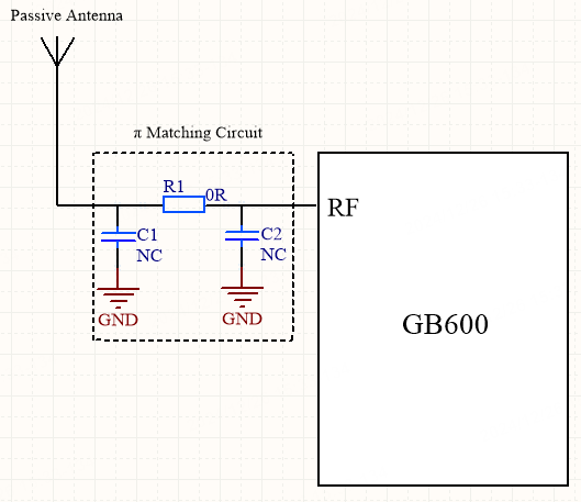
The preceding figure shows the circuit for connecting a standard passive antenna to the module. R1, C1, and C2 are reserved for impedance matching of the antenna. C1 and C2 are not connected by default, and the default resistance value of R1 is 0R. The impedance of the RF signal cable must be within 50Ω, and the trace needs to be as short as possible.
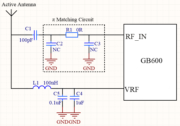
Active antenna reference design
The following figure shows the circuit for connecting a standard active antenna to the module. C1 is a DC-blocking capacitor. R1, C1, and C2 are reserved for impedance matching of the antenna. C1 and C2 are not connected by default, and the default resistance value of R1 is 0R. During PCB layout, L1, C4, and C5 must be placed close to the antenna interface, and the near end of the L1 pad should be connected to the RF trace.
Packing and production instructions
Mechanical dimensions
The following figure shows the mechanical dimensions of the GB600 module (unit: mm):
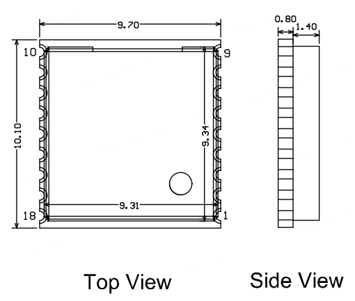
The default tolerance of the external dimensions of the module is ±0.35 mm, and the tolerance of key dimensions is ±0.1 mm. If you have special requirements for key dimensions, specify them in the datasheet after consultations.
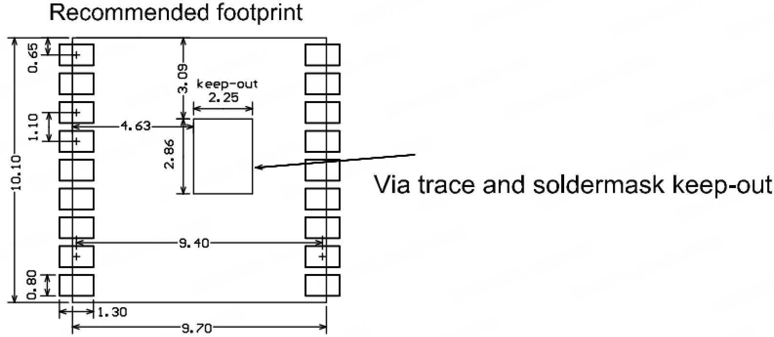
Bottom view and recommended footprint
The following figure shows the mechanical dimensions of the GB600 module in a bottom view (unit: mm):
The following figure shows the recommended footprint (unit: mm):
Production instructions
-
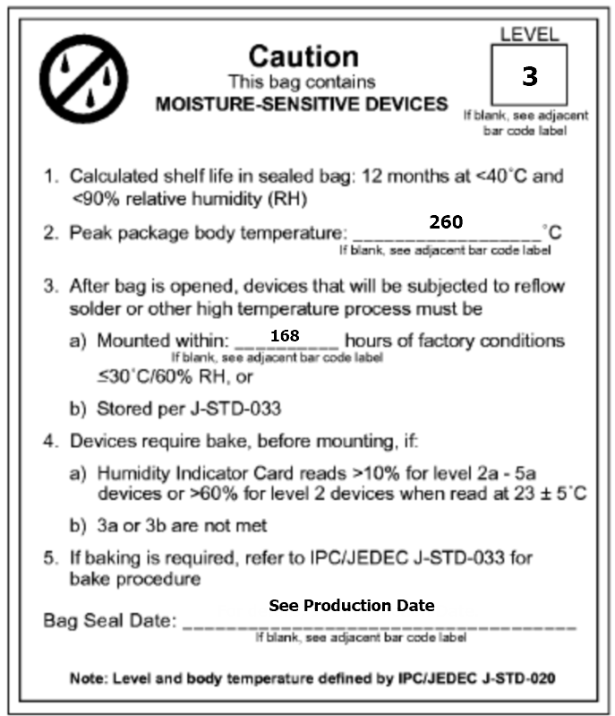
Package the module with the SMT if Tuya’s module is designed to be SMT-packaged. After being unpacked, the module must be soldered within 24 hours. Otherwise, it needs to be put into a drying cupboard with a relative humidity level no greater than 10%, or packaged in vacuum again. Then, record the packing time and duration of exposure. The total exposure time cannot exceed 168 hours.
- Instruments or devices required for the SMT process:
- Surface mount system
- SPI
- Reflow soldering machine
- Thermal profiler
- Automated optical inspection (AOI) device
- Instruments or devices required for the baking process:
- Cabinet oven
- Electrostatic discharge (ESD) protection and heat-resistant trays
- ESD protection and heat-resistant gloves
- Instruments or devices required for the SMT process:
-
A delivered module must meet the following storage requirements:
-
The moisture-proof bag must be placed in an environment where the temperature is below 40°C and the relative humidity is lower than 90%.
-
The shelf life of a dry-packaged product is 12 months from the date when the product is packaged and sealed.
-
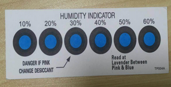
A humidity indicator card (HIC) is put in the sealed package.
-
-
The module needs to be baked in the following cases:
- The vacuum packaging bag is damaged before unpacking.
- After unpacking, no HIC is found in the packaging bag.
- After unpacking, the HIC indicates a humidity level of 10% or higher. In this case, the circle turns pink on the HIC.
- The total exposure time has lasted for over 168 hours since unpacking.
- More than 12 months have passed since the first sealing of the bag.
-
The baking parameter settings are described below:
- Baking temperature: 40°C for reel packaging with relative humidity ≤ 5%. And 125°C for tray packaging with relative humidity ≤ 5% (use a heat-resistant tray, rather than a plastic container).
- Baking time: 168 hours for reel packaging and 12 hours for tray packaging.
- Temperature for triggering an alert: 50°C for reel packaging and 135°C for tray packaging.
- Production can begin after a module has cooled down to below 36°C under natural conditions.
- If a module remains unused for over 168 hours after being baked, it needs to be baked again.
- If a batch of modules is not baked after exposure for more than 168 hours, do not use wave soldering to solder them. Because these modules are level-3 moisture-sensitive devices, they are very likely to get damp when exposed beyond the allowable time. In this case, if they are soldered at high temperatures, device failure or poor soldering performance might occur.
-
In the whole production process, take electrostatic discharge (ESD) protective measures.
-
To guarantee the pass rate, we recommend that you use the SPI and AOI to monitor the quality of solder paste printing and mounting.
Recommended oven temperature curve
Set the temperature according to the following temperature curve of reflow soldering. The peak temperature is 245°C.
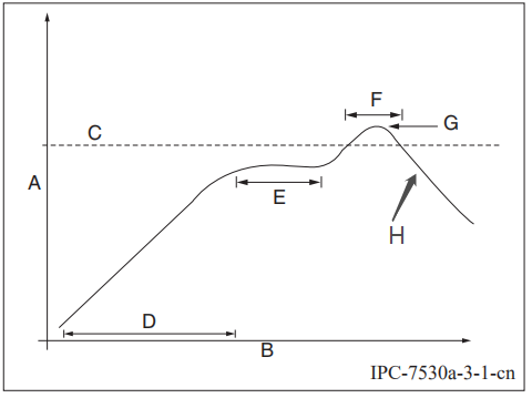
- A: temperature axis
- B: time axis
- C: alloy liquidus temperature from 217°C to 220°C
- D: ramp-up slope from 1°C/s to 3°C/s
- E: keep a constant temperature from 150°C to 200°C for a time period from 60s to 120s
- F: keep a temperature above liquidus temperature for 50s to 70s
- G: peak temperature from 235°C to 245°C
- H: ramp-down slope from 1°C/s to 4°C/s
The curve above is based on solder paste SAC305. For more information about other solder pastes, see the recommended oven temperature curve in the specified solder paste specifications.
Storage conditions
MOQ and packaging information
| Product model | MOQ (pcs) | Shipping packaging | Modules per reel | Reels per carton |
|---|---|---|---|---|
| GB600 | 4,800 | Tape and reel | 1,200 | 4 |
Is this page helpful?
YesFeedbackIs this page helpful?
YesFeedback


