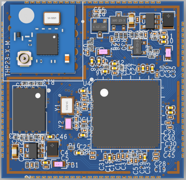
THP23-X-M Module Datasheet
Developed by Tuya, THP23-X-M is a core board for gateway development. It consists of a highly integrated smart high-definition display processor chip SSD202D and Tuya’s Wi-Fi module TY001. With rich peripheral interfaces, users can design peripheral circuits based on the core board for custom development. Moreover, if you have sufficient development capabilities, you can integrate with TuyaOS capabilities on top of THP23-X-M to meet more customization needs.
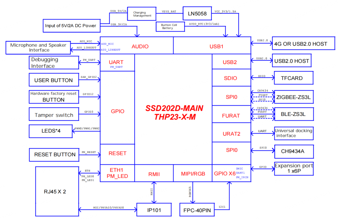
Demo block diagram
Features
- Operating voltage range: 3.14V to 3.46V
- Wi-Fi connectivity
- IEEE 802.11b/g/n20
- Channels 1–14@2.4 GHz (CH1–11 for US/CA and CH1–13 for EU/CN)
- Support security protocols, including WEP, WPA, WPA2, and WPA2 PSK (AES)
- The maximum output power is +19 dBm for IEEE 802.11b transmission
- Operating temperature range: 0°C to 70°C
- Microcontroller frequency: 1.2 GHz
- Abundant interfaces: 2 UART ports, 2 USB 2.0 ports, 2 RJ45 ports (one of which requires an external interface chip), MIC, SPK, MIPI, and other interfaces
Scope of applications
- Outdoor recreational vehicles and yachts
- New energy
- Agriculture
- Smart home
Module interfaces
| Pin | Symbol | Type | Description |
|---|---|---|---|
| 1 | SYS_3V3 | P | Power supply pin (3.3V). |
| 2 | GND1 | P | Ground pin. |
| 3 | WF_ANT | / | Radio frequency (RF) output. |
| 4 | GND2 | P | Ground pin. |
| 5 | GPIO4/PWM0 | I/O | GPIO pin, corresponding to P121 on the IC. This pin can be used as PWM0 output. |
| 6 | GPIO5/PWM1 | I/O | GPIO pin, corresponding to P122 on the IC. This pin can be used as PWM1 output. |
| 7 | GPIO6/I2C0_SCL | I/O | GPIO pin, corresponding to P123 on the IC. This pin can be used as I2C0 SCL. |
| 8 | GPIO7/I2C0_SDA | I/O | GPIO pin, corresponding to P124 on the IC. This pin can be used as I2C0 SDA. |
| 9 | GPIO8/UART2_RX/SPI0_CZ | I/O | GPIO pin, corresponding to P125 on the IC. This pin can be used as SPI0_CZ. |
| 10 | GPIO9/UART2_TX/SPI0_CK | I/O | GPIO pin, corresponding to P126 on the IC. This pin can be used as SPI0_CK. |
| 11 | GPIO10/SPI0_DI | I/O | GPIO pin, corresponding to P127 on the IC. This pin can be used as SPI0_DI. |
| 12 | GPIO11/SPI0_DO | I/O | GPIO pin, corresponding to P128 on the IC. This pin can be used as SPI0_DO. |
| 13 | GPIO12 | I/O | GPIO pin, corresponding to P1 on the IC. |
| 14 | GPIO13 | I/O | GPIO pin, corresponding to P2 on the IC. |
| 15 | GPIO14 | I/O | GPIO pin, corresponding to P3 on the IC. |
| 16 | GPIO85 | I/O | GPIO pin, corresponding to P5 on the IC. This pin can be used as UART2_RX. |
| 17 | GPIO86 | I/O | GPIO pin, corresponding to P6 on the IC. This pin can be used as UART2_TX. |
| 18 | DMIC_R | O | Digital microphone, right channel, corresponding to P7 on the IC. |
| 19 | DMIC_L | I/O | Digital microphone, left channel, corresponding to P8 on the IC. |
| 20 | DMIC_CLK | I | Digital microphone, clock, corresponding to P9 on the IC. |
| 21 | SAR_GPIO0 | I | GPIO pin, corresponding to P22 on the IC. This pin can be used as ADC. |
| 22 | SAR_GPIO2 | I | GPIO pin, corresponding to P21 on the IC. This pin can be used as ADC. |
| 23 | PM_IRIN | I | Infrared input, corresponding to P32 on the IC. |
| 24 | PM_RESET | I | System reset pin, corresponding to P33 on the IC. |
| 25 | PM_UART_RX | I | Debugging UART, input, corresponding to P34 on the IC. |
| 26 | PM_UART_TX | O | Debugging UART, output, corresponding to P35 on the IC. |
| 27 | GPIO47 | I/O | GPIO pin, corresponding to P36 on the IC. |
| 28 | GPIO48 | I/O | GPIO pin, corresponding to P37 on the IC. |
| 29 | UART1_RX | I | UART1 data input, corresponding to P38 on the IC. |
| 30 | UART1_TX | O | UART1 data output, corresponding to P39 on the IC. |
| 31 | FUART_RX | I | Fast UART data input, corresponding to P52 on the IC. |
| 32 | FUART_TX | O | Fast UART data output, corresponding to P53 on the IC. |
| 33 | FUART_CTS | I | Fast UART_CTS, flow control pin, corresponding to P54 on the IC. |
| 34 | FUART_RTS | O | Fast UART_RTS, flow control pin, corresponding to P55 on the IC. |
| 35 | GND3 | P | Ground pin. |
| 36 | TTL0 | O | LCD data interface, corresponding to P56 on the IC. |
| 37 | TTL1 | O | LCD data interface, corresponding to P57 on the IC. |
| 38 | TTL2 | O | LCD data interface, corresponding to P58 on the IC. |
| 39 | TTL3 | O | LCD data interface, corresponding to P59 on the IC. |
| 40 | TTL4 | O | LCD data interface, corresponding to P60 on the IC. |
| 41 | TTL5 | O | LCD data interface, corresponding to P61 on the IC. |
| 42 | GND4 | P | Ground pin. |
| 43 | TTL6/MIPI_TX_D0P | O | LCD data interface, corresponding to P65 on the IC. |
| 44 | TTL7/MIPI_TX_D0N | O | LCD data interface, corresponding to P66 on the IC. |
| 45 | TTL8/MIPI_TX_D1P | O | LCD data interface, corresponding to P67 on the IC. |
| 46 | TTL9/MIPI_TX_D1N | O | LCD data interface, corresponding to P68 on the IC. |
| 47 | TTL10/MIPI_TX_CKP | O | LCD data interface, corresponding to P69 on the IC. |
| 48 | TTL11/MIPI_TX_CKN | O | LCD data interface, corresponding to P70 on the IC. |
| 49 | TTL12/MIPI_TX_D2P | O | LCD data interface, corresponding to P71 on the IC. |
| 50 | TTL13/MIPI_TX_D2N | O | LCD data interface, corresponding to P72 on the IC. |
| 51 | TTL14/MIPI_TX_D3P | O | LCD data interface, corresponding to P73 on the IC. |
| 52 | TTL15/MIPI_TX_D3N | O | LCD data interface, corresponding to P74 on the IC. |
| 53 | GND5 | P | Ground pin. |
| 54 | TTL16 | O | LCD data interface, corresponding to P79 on the IC. |
| 55 | TTL17 | O | LCD data interface, corresponding to P80 on the IC. |
| 56 | TTL18 | O | LCD data interface, corresponding to P81 on the IC. |
| 57 | TTL19 | O | LCD data interface, corresponding to P82 on the IC. |
| 58 | TTL20 | O | LCD data interface, corresponding to P83 on the IC. |
| 59 | TTL21 | O | LCD data interface, corresponding to P84 on the IC. |
| 60 | TTL22 | O | LCD data interface, corresponding to P85 on the IC. |
| 61 | TTL23 | O | LCD data interface, corresponding to P86 on the IC. |
| 62 | TTL24 | O | LCD data interface, corresponding to P87 on the IC. |
| 63 | TTL25 | O | LCD data interface, corresponding to P88 on the IC. |
| 64 | TTL26 | O | LCD data interface, corresponding to P89 on the IC. |
| 65 | TTL27 | O | LCD data interface, corresponding to P90 on the IC. |
| 66 | GND6 | P | Ground pin. |
| 67 | SD_CDZ | I | Power management and insertion detection of the SD card, corresponding to P91 on the IC. |
| 68 | SD_D1 | I/O | SD card data interface, corresponding to P92 on the IC. |
| 69 | SD_D0 | I/O | SD card data interface, corresponding to P93 on the IC. |
| 70 | SD_CLK | O | SD card clock interface, corresponding to P94 on the IC. |
| 71 | SD_CMD | O | SD card command interface, corresponding to P95 on the IC. |
| 72 | SD_D3 | I/O | SD card data interface, corresponding to P96 on the IC. |
| 73 | SD_D2 | I/O | SD card data interface, corresponding to P97 on the IC. |
| 74 | GPIO0 | I/O | GPIO pin, corresponding to P99 on the IC. |
| 75 | GPIO1 | I/O | GPIO pin, corresponding to P100 on the IC. |
| 76 | GPIO2/I2C1_SCL | I/O | GPIO pin, corresponding to P101 on the IC. This pin can be used as IIC1_SCL. |
| 77 | GPIO3/I2C1_SDA | I/O | GPIO pin, corresponding to P102 on the IC. This pin can be used as IIC1_SDA. |
| 78 | PM_LED0 | O | Ethernet LED0 control pin, corresponding to P103 on the IC. |
| 79 | PM_LED1 | O | Ethernet LED1 control pin, corresponding to P104 on the IC. |
| 80 | GND7 | P | Ground pin. |
| 81 | ETH_RN | I | The receiver signal of 10/100M Ethernet differential pair, negative pole, corresponding to P107 on the IC. |
| 82 | ETH_RP | I | The receiver signal of 10/100M Ethernet differential pair, positive pole, corresponding to P108 on the IC. |
| 83 | ETH_TN | O | The transmitter signal of 10/100M Ethernet differential pair, negative pole, corresponding to P109 on the IC. |
| 84 | ETH_TP | O | The transmitter signal of 10/100M Ethernet differential pair, positive pole, corresponding to P110 on the IC. |
| 85 | GND8 | P | Ground pin. |
| 86 | DM_P1 | I/O | USB signal transmitting/receiving differential pair, negative pole, corresponding to P63 on the IC. |
| 87 | DP_P1 | I/O | USB signal transmitting/receiving differential pair, positive pole, corresponding to P62 on the IC. |
| 88 | DP_P2 | I/O | USB signal transmitting/receiving differential pair, positive pole, corresponding to P111 on the IC. |
| 89 | DM_P2 | I/O | USB signal transmitting/receiving differential pair, negative pole, corresponding to P112 on the IC. |
| 90 | GND9 | P | Ground pin. |
| 91 | AUD_LINEOUT_R0 | O | Audio right channel, output, corresponding to P115 on the IC. |
| 92 | AUD_LINEOUT_L0 | O | Audio left channel, output, corresponding to P116 on the IC. |
| 93 | AUD_MICCM0 | I | Audio left channel, microphone negative input, corresponding to P117 on the IC. |
| 94 | AUD_MICIN0 | I | Audio left channel, microphone positive input, corresponding to P118 on the IC. |
| 95 | GND10 | P | Ground pin. |
| 96 | AVDD_RTC | P | RTC power supply, 3.3V, corresponding to P64 on the IC. When in use, be sure to power this pin with a DC 3.3V power supply. |
Electrical parameters
Absolute electrical parameters
| Parameter | Description | Min value | Max value | Unit |
|---|---|---|---|---|
| Ts | Storage temperature | -20 | 85 | °C |
| VDD | Supply voltage | 2.97 | 3.6 | V |
Normal operating conditions
| Parameter | Description | Min value | Typical value | Max value | Unit |
|---|---|---|---|---|---|
| Ta | Operating temperature | -20 | / | 85 | °C |
| VCC | Operating voltage | 3.14 | 3.3 | 3.46 | V |
| VIL | I/O low-level input | / | 0 | 0.8 | V |
| VIH | I/O high-level input | 2.5 | 3.3 | / | V |
| VOL | I/O low-level output | / | 0 | 0.1 | V |
| VOH | I/O high-level output | VCC−0.1 | 3.3 | / | V |
Working mode and power consumption
The table below shows the power consumption performance of the THP23-X-M core board.
| Work mode | Operating voltage (V) | Average current (mA) | Peak current (mA) |
|---|---|---|---|
| Power-on | 3.29 | 263 | 760 |
| Pairing over Wi-Fi | 3.29 | 380 | 780 |
| Standby | 3.29 | 295 | 580 |
| Disconnected | 3.29 | 318 | 1020 |
RF parameters
For more information, see TY001 Module Datasheet.
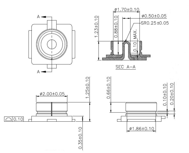
Antenna information
Antenna type
The board can be connected to an external antenna through the half hole on the module, or to an IPEX antenna with the onboard IPEX connector. You can choose either one of the two.
Antenna interference reduction
The distance between the antenna and other mental components should be at least 15 mm to provide the best Wi-Fi performance.
Specifications of antenna connector
Packing and production instructions
Mechanical dimensions and packing
Mechanical dimensions of the THP23-X-M PCB are 35±0.35 mm (W) × 34±0.35 mm (L) × 2.9±0.1 mm (H). The figure below shows the mechanical dimensions of THP23-X-M.
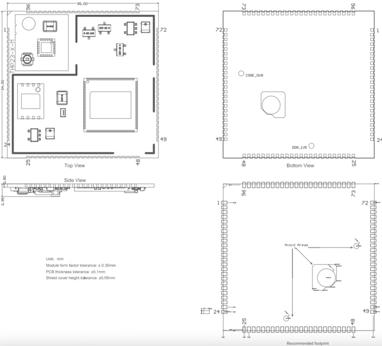
The default dimensional tolerance is ±0.35 mm. If you have special requirements for key dimensions, specify them in the datasheet after consultations.
Production instructions
-
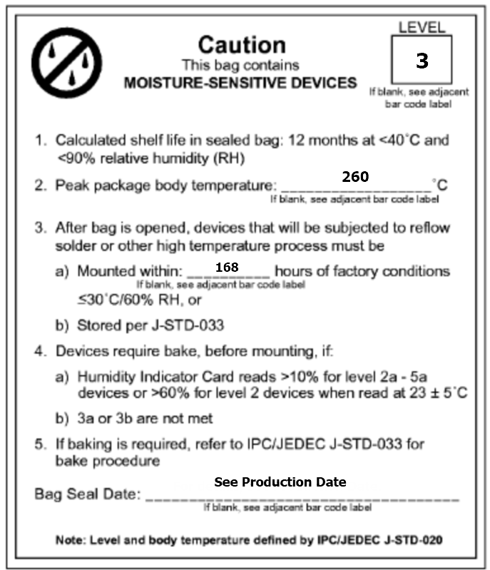
Package the module with the SMT if Tuya’s module is designed to be SMT-packaged. After being unpacked, the module must be soldered within 24 hours. Otherwise, it needs to be put into a drying cupboard with a relative humidity level no greater than 10%, or pack the module in vacuum again. Then, record the packing time and duration of exposure. The total exposure time cannot exceed 168 hours.
- Instruments or devices required for the SMT process:
- Surface mount system
- SPI
- Reflow soldering machine
- Thermal profiler
- AOI
- Instruments or devices required for the baking process:
- Cabinet oven
- Anti-electrostatic and heat-resistant trays
- Anti-electrostatic and heat-resistant gloves
- Instruments or devices required for the SMT process:
-
A delivered module must meet the following storage requirements:
-
The moisture-proof bag must be placed in an environment where the temperature is below 40°C and the relative humidity is lower than 90%.
-
The shelf life of a dry-packaged product is 12 months from the date when the product is packaged and sealed.
-
A humidity indicator card (HIC) is put in the sealed package.
-
-
The module needs to be baked in the following cases:
- The vacuum packaging bag is damaged before unpacking.
- After unpacking, no HIC is found in the packaging bag.
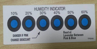
- After unpacking, the HIC indicates a humidity level of 10% or higher. In this case, the circle turns pink on the HIC.
- The total exposure time has lasted for over 168 hours since unpacking.
- More than 12 months have passed since the first sealing of the bag.
-
The baking parameter settings are described below:
- Baking temperature: 40°C for reel packaging with relative humidity ≤ 5%. And 125°C for tray packaging with relative humidity ≤ 5% (use the heat-resistant tray, rather than plastic containers).
- Baking time: 168 hours for reel packaging and 12 hours for tray packaging.
- Temperature for triggering an alert: 50°C for reel packaging and 135°C for tray packaging.
- Production can begin after a module has cooled down to below 36°C under natural conditions.
- If a module remains unused for over 168 hours after being baked, it needs to be baked again.
- If a batch of modules is not baked after exposure for more than 168 hours, do not use wave soldering to solder them. Because these modules are level-3 moisture-sensitive devices, they are very likely to get damp when exposed beyond the allowable time. In this case, if they are soldered at high temperatures, device failure or poor soldering performance might occur.
-
In the whole production process, take electrostatic discharge (ESD) protective measures.
-
To guarantee the pass rate, we recommend that you use the SPI and AOI to monitor the quality of solder paste printing and mounting.
Recommended oven temperature curve
Set the temperature according to the following temperature curve of reflow soldering. The peak temperature is 245°C.
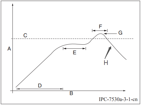
-
A: temperature axis
-
B: time axis
-
C: alloy liquidus temperature from 217°C to 220°C
-
D: ramp-up slope from 1°C/s to 3°C/s
-
E: keep a constant temperature from 150°C to 200°C for a time period from 60s to 120s
-
F: temperature above liquidus temperature for 50s to 70s
-
G: peak temperature from 235°C to 245°C
-
H: ramp-down slope from 1°C/s to 4°C/s
The curve above is based on solder paste SAC305. For more information about other solder pastes, see the recommended oven temperature curve in the specified solder paste specifications.
Storage conditions
MOQ and packaging information
| Product model | MOQ (pcs) | Shipping packaging |
|---|---|---|
| THP23-X-M | 500 | Tape and reel |
Is this page helpful?
YesFeedbackIs this page helpful?
YesFeedback


