ZS3L Module Datasheet
ZS3L is a Zigbee module that Tuya has developed. It consists of a highly integrated RF processor chip (EFR32MG21A020F768IM32-B) and several peripheral components, with an embedded 802.15.4 PHY/MAC Zigbee network protocol stack and robust library functions.
Overview
ZS3L is embedded with a 32-bit low-power Arm Cortex-M33 core, 768-KB flash memory, and 64-KB RAM, and has rich peripherals.
ZS3L integrates all function libraries of the Zigbee MAC. You can develop embedded Zigbee products as required.
Features
- Embedded low-power 32-bit Arm Cortex-M33 processor, which provides a digital signal processor (DSP) instructions and floating-point units (FPUs) and can also function as an application processor
- Clock rate: 80 MHz
- Operating voltage: 2.0 to 3.8 V
- Peripherals: 9×GPIOs, 1×UART, 1×ADC
- Zigbee Connectivity
- 802.15.4 MAC/PHY
- Channels 11 - 26@2.400-2.483GHz, 250 Kbit/s air interface rate
- Maximum output power: +20 dBm
- Runtime power consumption: 60 µA/MHz; current in sleep mode: 5 µA
- Onboard PCB antenna with a gain of 1.0 dBi
- Operating temperature: –40℃ to +105℃
- AES 128/256 hardware encryption
Applications
- Intelligent building
- Smart household and home appliances
- Smart socket and light
- Industrial wireless control
- Baby monitor
- Network camera
- Intelligent bus
Module interfaces
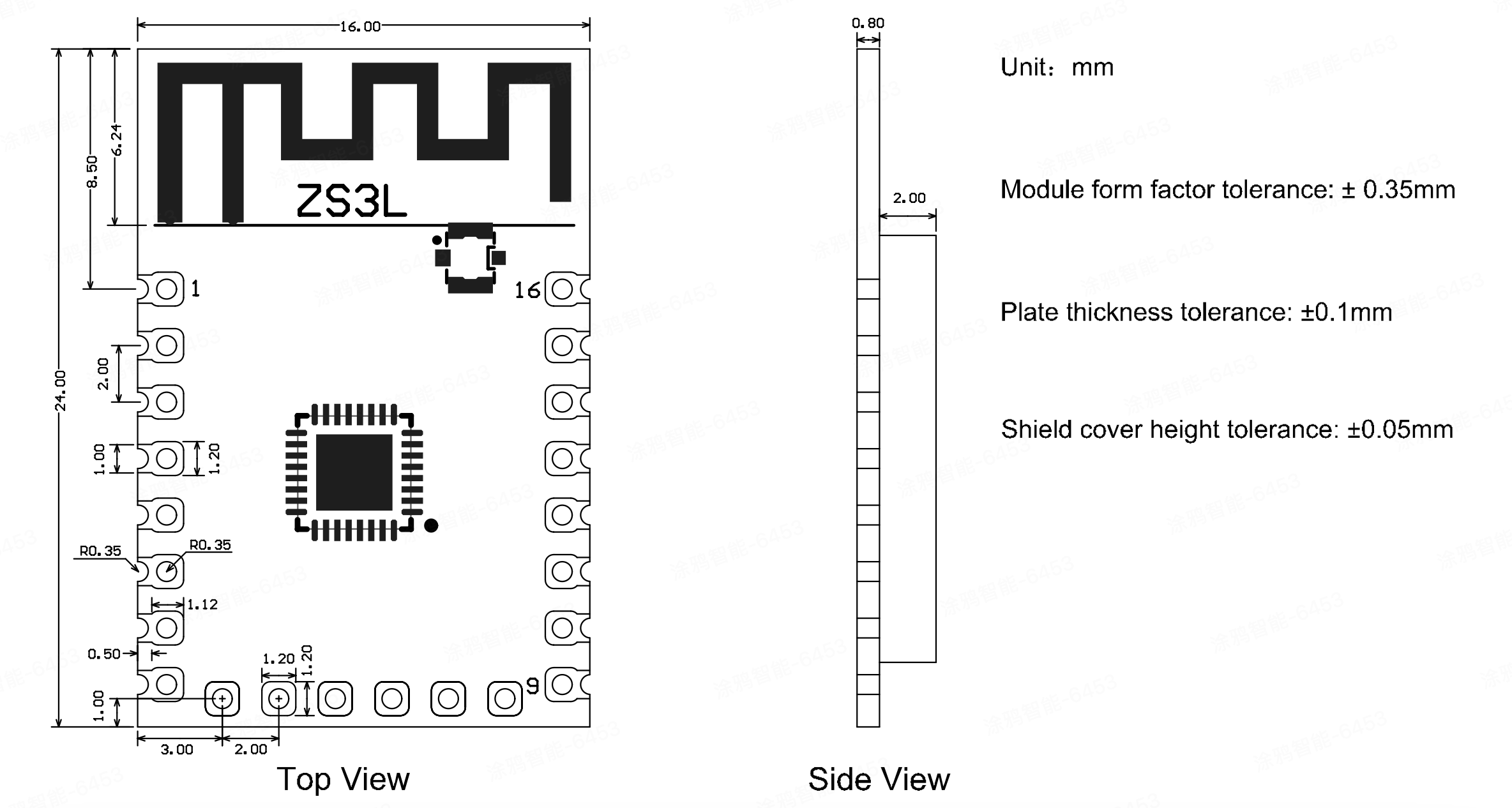
Dimensions and footprint
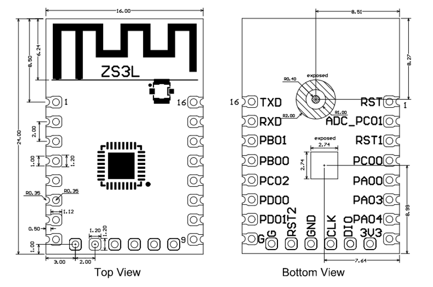
ZS3L has two lines of pins with a spacing of 2±0.1 mm.
The ZS3L dimensions (H x W x L) are 2.8±0.15 mm x 24±0.35 mm x 16±0.35 mm. Figure 2-1 shows the ZS3L front and rear views.
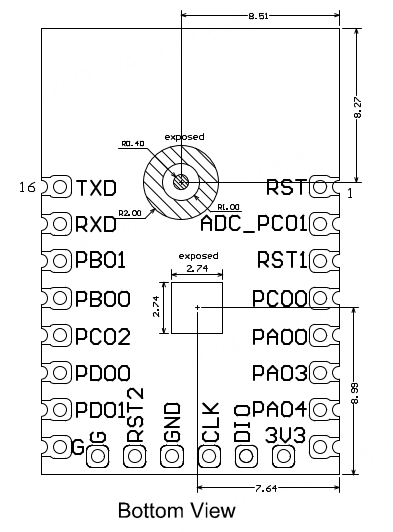
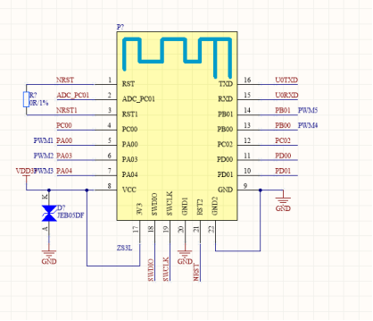
Interface pin definition
| No. | Symbol | Type | Function |
|---|---|---|---|
| 1 | RST | I | Hardware reset pin, which is at a high level by default and is active at a low level |
| 2 | ADC_PC01 | I/O | 12-bit SAR ADC pin |
| 3 | RST1 | I | Disconnected, which can be used as the reset pin in special scenarios |
| 4 | PC00 | I/O | Hardware PWM pin, which is connected to PC00 (pin 1) on the internal IC |
| 5 | PA00 | I/O | Hardware PWM pin, which is connected to PA00 (pin 17) on the internal IC |
| 6 | PA03 | I/O | Hardware PWM pin, which is connected to PA03 (pin 20) on the internal IC |
| 7 | PA04 | I/O | Hardware PWM pin, which is connected to PA04 (pin 21) on the internal IC |
| 8 | 3V3 | P | Power supply pin (typical power supply voltage: 3.3 V) |
| 9 | GND | P | Power supply reference ground pin |
| 10 | PD01 | I/O | Hardware PWM pin, which is connected to PD01 (pin 31) on the internal IC |
| 11 | PD00 | I/O | Hardware PWM pin, which is connected to PD00 (pin 32) on the internal IC |
| 12 | PC02 | I/O | Hardware PWM pin, which is connected to PC02 (pin 3) on the internal IC |
| 13 | PB00 | I/O | Hardware PWM pin, which is connected to PB00 (pin 16) on the internal IC |
| 14 | PB01 | I/O | Hardware PWM pin, which is connected to PB01 (pin 15) on the internal IC |
| 15 | RXD | I/O | UART_RXD, which is connected to PA06 (pin 23) on the internal IC |
| 16 | TXD | I/O | UART_TXD, which is connected to PA05 (pin 22) on the internal IC |
| 17 | 3V3 | P | Power supply pin (typical power supply voltage: 3.3 V) |
| 18 | DIO | I/O | J-Link SWDIO programming pin |
| 19 | CLK | I/O | J-Link SWCLK programming pin |
| 20 | GND1 | P | Power supply reference ground pin |
| 21 | RST2 | I/O | Hardware reset pin, which is at a high level by default and is active at a low level |
| 22 | GND2 | P | Power supply reference ground pin |
Note:
- P indicates a power supply pin, and I/O indicates an input/output pin.
- Pin 17-22 are burning pins, which are not exposed by default. During routing, you should avoid them.
When the ZS3L is used as a gateway module, its pins should be connected as follows:
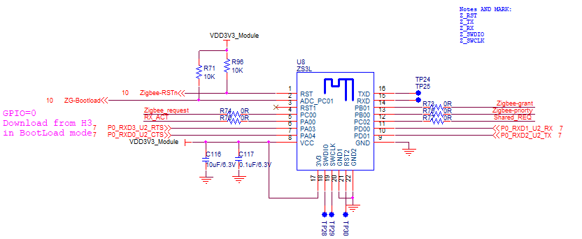
| Pin name printed on the module | Corresponding pin when used as a gateway module | Pin on the internal IC | Remarks |
|---|---|---|---|
| PA03 | UART_CTS | PA03 | The coordinator used for the gateway must be connected to hardware flow control by default. The baud rate is 115200. The pin is connected to UART_RTS of the MCU. |
| PA04 | UART_RTS | PA04 | The coordinator used for the gateway must be connected to hardware flow control by default. The baud rate is 115200. The pin is connected to UART_CTS of the MCU. |
| PD00 | UART_TX | PD00 | The pin is connected to UART_RX of the MCU. |
| PD01 | UART_RX | PD01 | The pin is connected to UART_TX of the MCU. |
| RST | RST | RST | The pin is connected to the GPIO of the MCU, and the GPIO is at high level by default. |
| PC00 | REQUEST | PC00 | The pin is connected to STATE of the MCU, and the PTA pin needs to be connected to a 1.5-K pull-down resistor. |
| PB01 | GRANT | PB01 | The pin is connected to ACT of the MCU. |
| PB00 | PRIORITY | PB00 | The pin is connected to PRI of the MCU, and the PTA pin needs to be connected to a 1.5-K pull-down resistor. |
| PC02 | Shared_REQ | PC02 | This pin needs to be connected to a 1.5-K pull-down resistor. Connect to Shared_REQ of the BT. |
| PA00 | RX_ACT | PA00 | This pin needs to be connected to a 1.5-K pull-down resistor. Connect to RX_ACT of the BT. |
| ADC_PC01 | Bootload | PC01 | The module enters Bootloader mode if the pin is held low during reset (RST). |
Note: The 1.5-K pull-down resistor is required whether it is used by a single module or not.
Electrical parameters
Absolute electrical parameters
| Parameter | Description | Minimum value | Maximum value | Unit |
|---|---|---|---|---|
| Ts | Storage temperature | -50 | 150 | ℃ |
| VBAT | Power supply voltage | 2.0 | 3.8 | V |
| ESD voltage (human body model) | TAMB-25℃ | - | 2 | KV |
| ESD voltage (machine model) | TAMB-25℃ | - | 0.5 | KV |
Working conditions
| Parameter | Description | Minimum value | Average value | Maximum value (Typical value) | Unit |
|---|---|---|---|---|---|
| Ta | Operating temperature | -40 | - | 105 | ℃ |
| VCC | Supply voltage | 2.0 | 3.0 | 3.8 | V |
| VIL | I/O low-level input | - | - | IOVDD*0.3 | V |
| VIH | I/O high-level input | IOVDD*0.7 | - | - | V |
| VOL | I/O low-level output | - | - | IOVDD*0.2 | V |
| VOH | I/O high-level output | IOVDD*0.8 | - | - | V |
Current consumption during constant transmission and receiving
| Working status | Mode | Rate | TX Power/ Receiving | Typical value | Maximum value | Unit |
|---|---|---|---|---|---|---|
| TX | - | 250 Kbit/s | +20dBm | 200 | 206 | mA |
| TX | - | 250 Kbit/s | +10dBm | 62 | 64 | mA |
| TX | - | 250 Kbit/s | +0dBm | 26 | 28 | mA |
| RX | - | 250 Kbit/s | Constant receiving | 10 | 12 | mA |
| RX | - | 250 Kbit/s | Constant receiving | 10 | 12 | mA |
| RX | - | 250 Kbit/s | Constant receiving | 10 | 12 | mA |
Operating current
| Working mode | Working status (Ta = 25℃) | Average value | Maximum value | Unit |
|---|---|---|---|---|
| EZ | The module is in EZ mode. | 10 | 40 | mA |
| Connected and idle | The module is connected to the network and in idle state. | 11 | 13 | mA |
| Connected and busy | The module is connected to the network and in running state. | 12 | 66 | mA |
| Deep sleep mode | The module is in deep sleep mode, with 64 KB flash memory. | 5 | - | μA |
RF features
Basic RF features
| Parameter | Description |
|---|---|
| Frequency band | 2.405-2.480GHz |
| Zigbee standard | IEEE 802.15.4 |
| Data transmission rate | 250 Kbit/s |
| Antenna type | PCB antenna with a gain of 1 dBi |
TX performance
Performance during constant transmission
| Parameter | Minimum value | Typical value | Maximum value | Unit |
|---|---|---|---|---|
| Maximum output power(250Kbps) | - | 20 | - | dBm |
| Minimum output power(250Kbps) | - | -30 | - | dBm |
| Output power adjustment step | - | 0.5 | 1 | dBm |
| Output spectrum adjacent-channel rejection ratio | - | -31 | - | dBc |
| Frequency error | -15 | - | 15 | ppm |
RX performance
RX sensitivity
| Parameter | Minimum value | Typical value | Maximum value | Unit |
|---|---|---|---|---|
| PER<8%, RX sensitivity(250Kbps) | -102 | -101 | -99 | dBm |
Antenna
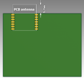
Antenna type
ZS3L uses an onboard PCB antenna.
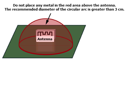
Antenna interference reduction
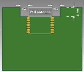
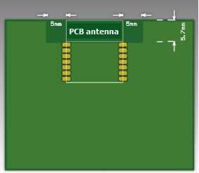
To ensure optimal Zigbee performance when the Zigbee module uses an onboard PCB antenna, it is recommended that the antenna be at least 5 mm away from other metal parts.
To prevent an adverse impact on the antenna radiation performance, avoid copper or traces along the antenna area on the PCB.
Packaging and production instructions
Mechanical dimensions
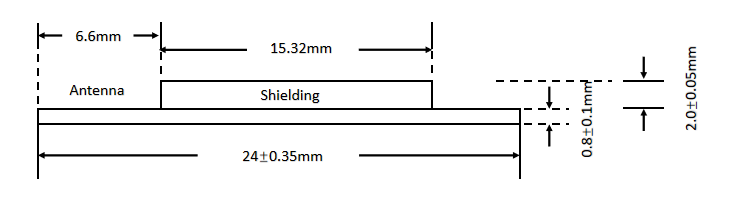
The PCB dimensions (H x W x L) are 0.8±0.1 mm x 24±0.35 mm x 16±0.35 mm.
Side view
Recommended schematic encapsulation
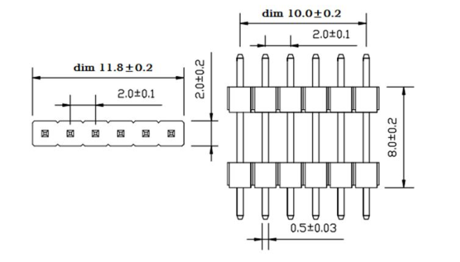
Recommended PCB footprint-Pin header
ZS3L can be mounted onto a PCB by using an SMT placement machine or through-hole mounted onto the PCB through a pin header. Figure 6-4 shows the pin header dimensions.
Recommended PCB footprint-SMT
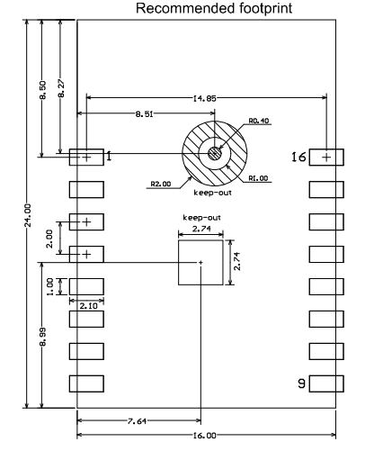
The area indicated as keep-out in the diagram above does not require tinning and should not have any traces routed through it.
Production instructions
-
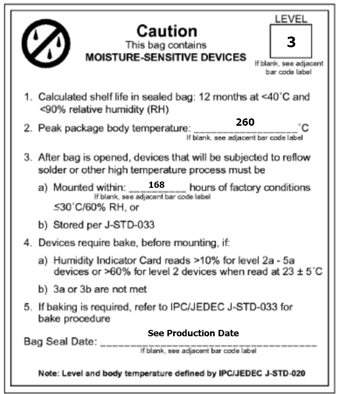
For the modules that can be packaged with the SMT or in an in-line way, you can select either of them according to the PCB design solutions of customers. If a PCB is designed to be SMT-packaged, package the module with the SMT. If a PCB is designed to be in-line-packaged, package the module in an in-line way. After being unpacked, the module must be soldered within 24 hours. Otherwise, it needs to be put into the drying cupboard where the relative humidity is not greater than 10%; or it needs to be packaged again under vacuum and the exposure time needs to be recorded (the total exposure time cannot exceed 168 hours).
- (SMT process) SMT devices:
- Mounter
- SPI
- Reflow soldering machine
- Thermal profiler
- Automated optical inspection (AOI) equipment
- Baking devices:
- Cabinet oven
- Anti-electrostatic and heat-resistant trays
- Anti-electrostatic and heat-resistant gloves
- (SMT process) SMT devices:
-
Storage conditions for a delivered module:
-
The moisture-proof bag must be placed in an environment where the temperature is below 40°C and the relative humidity is lower than 90%.
-
The shelf life of a dry-packaged product is 12 months from the date when the product is packaged and sealed.
-
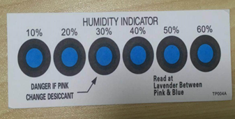
There is a humidity indicator card (HIC) in the packaging bag.
-
-
The module needs to be baked in the following cases:
- The packaging bag is damaged before unpacking.
- There is no humidity indicator card (HIC) in the packaging bag.
- After unpacking, circles of 10% and above on the HIC become pink.
- The total exposure time has lasted for over 168 hours since unpacking.
- More than 12 months have passed since the sealing of the bag.
-
Baking settings:
- Temperature: 40°C and ≤ 5% RH for reel package and 125°C and ≤5% RH for tray package (please use the heat-resistant tray rather than plastic container)
- Time: 168 hours for the reel package and 12 hours for tray package
- Alarm temperature: 50°C for reel package and 135°C for tray package
- Production-ready temperature after natural cooling: < 36°C
- Re-baking situation: If a module remains unused for over 168 hours after being baked, it needs to be baked again.
- If a batch of modules is not baked within 168 hours, do not use reflow soldering or wave soldering to solder them. Because these modules are Level-3 moisture-sensitive devices, they are very likely to get damp when exposed beyond the allowable time. In this case, if they are soldered at high temperatures, it may result in device failure or poor soldering.
-
In the whole production process, take electrostatic discharge (ESD) protective measures.
-
To guarantee the passing rate, it is recommended that you use the SPI and AOI to monitor the quality of solder paste printing and mounting.
Recommended oven temperature curve
Select a proper soldering manner according to the process. For the SMT process, please refer to the recommended oven temperature curve of reflow soldering. For the wave soldering process, please refer to the recommended oven temperature curve of wave soldering. There are some differences between the set temperatures and the actual temperatures. All the temperatures shown in this module datasheet are obtained through actual measurements.
Manner 1: SMT process (Recommended oven temperature curve of reflow soldering)
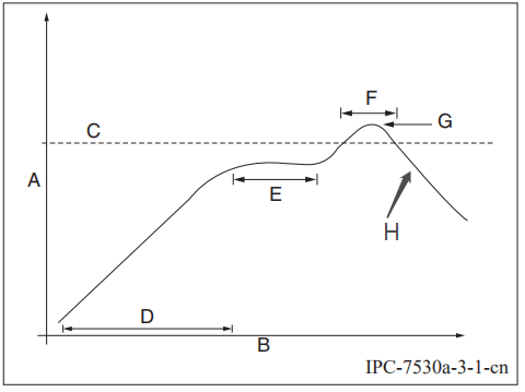
Set oven temperatures according to the following curve.
-
A: Temperature axis
-
B: Time axis
-
C: Liquidus temperature: 217 to 220°C
-
D: Ramp-up slope: 1 to 3°C/s
-
E: Duration of constant temperature: 60 to 120s; the range of constant temperature: 150 to 200°C
-
F: Duration above the liquidus: 50 to 70s
-
G: Peak temperature: 235 to 245°C
-
H: Ramp-down slope: 1 to 4°C/s
Note: The above curve is just an example of the solder paste SAC305. For more details about other solder pastes, please refer to Recommended oven temperature curve in the solder paste specifications.
Manner 2: Wave soldering process (Oven temperature curve of wave soldering)
Set oven temperatures according to the following temperature curve of wave soldering. The peak temperature is 260°C±5°C.
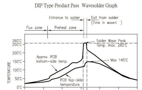
| Suggestions on oven temperature curve of wave soldering | Suggestions on manual soldering temperature | ||
|---|---|---|---|
| Preheat temperature | 80 to 130 °C | Soldering temperature | 360±20°C |
| Preheat time | 75 to 100s | Soldering time | <3s/point |
| Peak contact time | 3 to 5s | NA | NA |
| Temperature of tin cylinder | 260±5°C | NA | NA |
| Ramp-up slope | ≤2°C/s | NA | NA |
| Ramp-down slope | ≤6°C/s | NA | NA |
Storage conditions
MOQ and packing
| Product model | MOQ(pcs) | Packing method | Number of Modules in each reel pack | Number of reel packs in each box |
|---|---|---|---|---|
| ZS3L | 3600 | Tape reel | 900 | 4 |
Appendix: Statement
FCC Caution: Any changes or modifications not expressly approved by the party responsible for compliance could void the user’s authority to operate this equipment.
This device complies with Part 15 of the FCC Rules. Operation is subject to the following two conditions: (1) This device may not cause harmful interference, and (2) this device must accept any interference received, including interference that may cause undesired operation.
Note: This equipment has been tested and found to comply with the limits for a Class B digital device, according to part 15 of the FCC Rules. These limits are designed to provide reasonable protection against harmful interference in a residential installation. This equipment generates, uses, and can radiate radio frequency energy and, if not installed and used following the instructions, may cause harmful interference to radio communications. However, there is no guarantee that interference will not occur in a particular installation. If this equipment does cause harmful interference to radio or television reception, which can be determined by turning the equipment off and on, the user is encouraged to try to correct the interference by one or more of the following measures:
- Reorient or relocate the receiving antenna.
- Increase the separation between the equipment and the receiver.
- Connect the equipment to an outlet on a circuit different from that to which the receiver is connected.
- Consult the dealer or an experienced radio/TV technician for help.
Radiation Exposure Statement
This equipment complies with FCC radiation exposure limits set forth for an uncontrolled rolled environment. This equipment should be installed and operated with a minimum distance of 20cm between the radiator and your body.
Important Note
This radio module must not be installed to co-locate and operate simultaneously with other radios in the host system except by following FCC multi-transmitter product procedures. Additional testing and equipment authorization may be required to operate simultaneously with other radios.
The availability of some specific channels and/or operational frequency bands are country dependent and are firmware programmed at the factory to match the intended destination. The firmware setting is not accessible by the end-user.
The host product manufacturer is responsible for compliance with any other FCC rules that apply to the host not covered by the modular transmitter grant of certification. The final host product still requires Part 15 Subpart B compliance testing with the modular transmitter installed.
The end-user manual shall include all required regulatory information/warning as shown in this manual, including This product must be installed and operated with a minimum distance of 20 cm between the radiator and user body.
This device has got an FCC ID: 2ANDL-ZS3L. The end product must be labeled in a visible area with the following: "Contains Transmitter Module FCC ID: 2ANDL-ZS3L"
This device is intended only for OEM integrators under the following conditions:
-
The antenna must be installed such that 20cm is maintained between the antenna and users, and
-
The transmitter module may not be co-located with any other transmitter or antenna.
As long as the 2 conditions above are met, further transmitter tests will not be required. However, the OEM integrator is still responsible for testing their end-product for any additional compliance requirements required with this module installed.
Declaration of Conformity European notice

Hereby, Hangzhou Tuya Information Technology Co., Ltd declares that this module product complies with essential requirements and other relevant provisions of Directive 2014/53/EU,2011/65/EU. A copy of the Declaration of conformity can be found at https://www.tuya.com

This product must not be disposed of as normal household waste, following the EU directive for waste electrical and electronic equipment (WEEE- 2012/19/EU). Instead, it should be disposed of by returning it to the point of sale, or a municipal recycling collection point.
The device could be used with a separation distance of 20cm from the human body.
Is this page helpful?
YesFeedbackIs this page helpful?
YesFeedback


