JWBR2S-3.3V Module Datasheet
Last Updated on : 2025-05-29 06:20:23download
Product Overview
Developed by Tuya, JWBR2S-3.3V is a WiFi module that is suitable for serial communication of the 3.3 V TTL level. It consists of dual modules: WiFi module+Bluetooth WBR1 module, and a level conversion circuit. It’s further embedded with the Wi-Fi/BT network protocol stack and serial communication protocol
JWBR2S-3.3V is an RTOS platform. On the basis of the connection manner of serial communication, you can develop embedded products as required.
Features
- Embedded low-power KM4-MCU, which can also function as an application processor
- The maximum clock rate: 100 MHz
- Working voltage: 3.3 V
- Peripherals: 1 universal asynchronous receiver/transmitter (UART)
- WiFi connectivity
- 802.11 b/g/n20
- Channels 1 to 14 at 2.4 Ghz
- Support Bluetooth LE (Bluetooth Low Energy) 4.2
- Support WPA and WPA 2 security modes
- Up to +18 dBm output power in 802.11b mode
- Support SmartConfig functions for Android and iOS devices
- Onboard PCB antenna
- Working temperature: -20℃ to 85℃
Applications
- Intelligent building
- Smart household and home appliances
- Smart socket and light
- Industrial wireless control
- Baby monitor
- Network camera
- Intelligent bus
Change History
| Serial Number | Update Date | Updated Content | Version after Update |
|---|---|---|---|
| 1 | 2/26/2020 | This is the first release. | V2.0.0 |
Module Interfaces
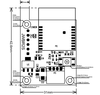
Dimensions and Footprint
The electrical interface of JWBR2S-3.3V is the PH-4AW connector with a spacing of 2.0 mm.
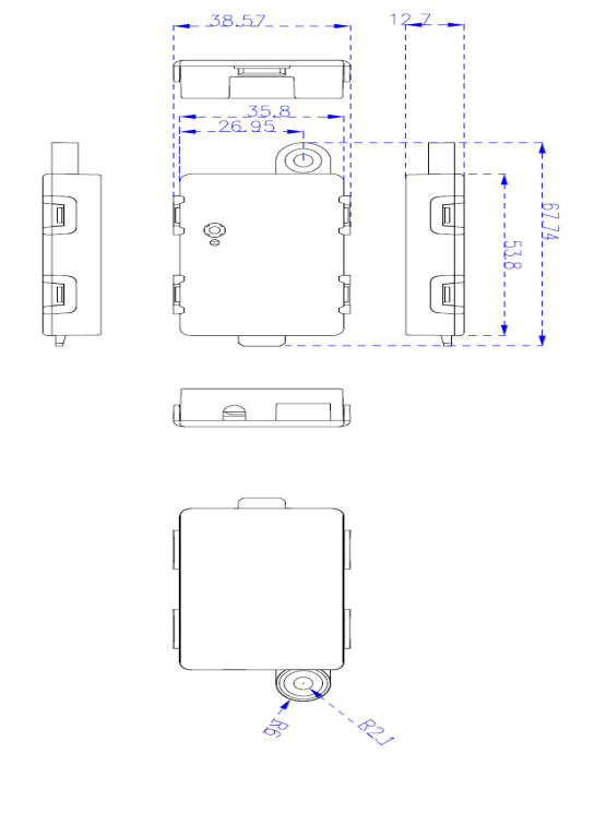
As shown in the following figure, the dimensions of JWBR2S-3.3V are 42.6±0.35 mm (L)×31±0.35 mm (W) ×9.1±0.15 mm (H). The thickness of the PCB is 1.2±0.1 mm.
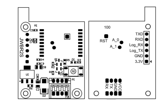
Pin Definition
| Pin Number | Symbol | I/O Type | Function |
|---|---|---|---|
| 1 | RX | I/O | UART0_RXD, receiver for communication of the module, input the level of 3.3V TTL |
| 2 | TX | I/O | UART0_TXD, transmitter for communication of the module, output the level of 3.3V TTL |
| 3 | GND | P | Power supply reference ground |
| 4 | VCC | P | Power supply pin (3.3V) |
Note: P indicates power supply pins and I/O indicates input/output pins.
Definitions on Test Points
| Pin Number | Symbol | I/O Type | Function |
|---|---|---|---|
| 1 | 3.3V | P | Power supply pin inside the module (3.3V) |
| 2 | GND | P | Power supply reference ground |
| 3 | Log_Tx | I/O | UART_Log_TXD (used to display the internal information of the module) |
| 4 | Log_Rx | I/O | UART_Log_RXD (used to display the internal information of the module) |
| 5 | RXD | I/O | Programming interface for firmware of the module |
| 6 | TXD | I/O | Programming interface for firmware of the module |
| 7 | A_0 | I/O | GPIOA_0, programming interface for firmware of the module During download, the pin needs to be pulled to 3.3V. |
| 8 | RST | I/O | Hardware reset pin |
Note: P indicates power supply pins, I/O indicates input/output pins and test points are prohibited.
Electrical Parameters
Absolute Electrical Parameters
| Parameter | Description | Minimum value | Maximum Value | Unit |
|---|---|---|---|---|
| Ts | Storage temperature | -40 | 105 | ℃ |
| VBAT | Power supply voltage | -0.3 | 3.3 | V |
| Static electricity discharge voltage (human body model) | TAMB-25℃ | - | 2 | KV |
| Static electricity discharge voltage (machine model) | TAMB-25℃ | - | 0.5 | KV |
Normal Working Conditions
| Parameter | Description | Minimum value | Typical Value | Maximum Value | Unit |
|---|---|---|---|---|---|
| Ta | Working temperature | -20 | - | 85 | ℃ |
| VBAT | Power supply voltage | 3.0 | 3.3 | 3.6 | V |
| VIL | IO low-level input | -0.3 | - | VCC*0.25 | V |
| VIH | IO high-level input | VCC*0.75 | - | VCC | V |
| VOL | IO low-level output | - | - | VCC*0.1 | V |
| VOH | IO high-level output | VCC*0.8 | - | VCC | V |
| Imax | IO drive current | - | - | 16 | mA |
| Cpad | Input pin capacitance | - | 2 | - | pF |
TX Power Consumption:
| Working Status | Mode | Rate | Transmit Power | Average Value | Peak Value (Typical Value)) | Unit |
|---|---|---|---|---|---|---|
| Transmit | 11b | 11Mbps | +17 dBm | 217 | 268 | mA |
| Transmit | 11b | 11Mbps | +18 dBm | 225 | 280 | mA |
| Transmit | 11 g | 54Mbps | +15 dBm | 159 | 188 | mA |
| Transmit | 11 g | 54Mbps | +17.5 dBm | 177 | 213 | mA |
| Transmit | 11n BW20 | MCS7 | +13 dBm | 145 | 167 | mA |
| Transmit | 11n BW20 | MCS7 | +16.5 dBm | 165 | 193 | mA |
RX power consumption:
| Working Status | Mode | Receive | Average Value | Peak Value (Typical Value)) | Unit |
|---|---|---|---|---|---|
| Receive | CPU Sleep | 11Mbps | 63 | 75 | mA |
| Receive | CPU Active | 54Mbps | 65 | 78 | mA |
| Receive | CPU Active | MCS7 | 65 | 78 | mA |
Power Consumption in Working Mode
| Working Mode | Working Status, Ta = 25°C | Average Value | Peak Value (Typical Value) | Unit |
|---|---|---|---|---|
| Quick connection network state | The module is in the fast network connection state | 74 | 324 | mA |
| Network connection idle state | The module is in the network connection idle state | 62 | 320 | mA |
| Network connection operation state | The module is connected to the network | 65 | 315 | mA |
| Disconnected state | The module is disconnected | 66 | 322 | mA |
Note: The peak lasts about 5us. The above parameters may vary with different firmware functions.
RF Parameters
Basic RF Features
| Parameter | Description |
|---|---|
| Working frequency | 2.400 to 2.484GHz |
| WiFi standard | IEEE 802.11 b/g/n (channels 1 to 14) |
| Data transmission rate | 11b: 1, 2, 5.5, 11 (Mbps); 11g: 6, 9, 12, 18, 24, 36, 48, 54 (Mbps); 11n: HT20 MCS 0 to 7 |
| Antenna type | IPEX Antenna |
TX Performance
TX performance
| Parameter | Minimum Value | Typical Value | Maximum Value | Unit |
|---|---|---|---|---|
| Average RF output power, 802.11b CCK Mode 11M | - | 17.5 | - | dBm |
| Average RF output power, 802.11g OFDM Mode 54M | - | 14.5 | - | dBm |
| Average RF output power, 802.11n OFDM Mode MCS7 | - | 13.5 | - | dBm |
| Frequency error | -20 | - | 20 | ppm |
RX Performance
RX sensitivity
| Parameter | Minimum Value | Typical Value | Maximum Value | Unit |
|---|---|---|---|---|
| PER<8%, RX sensitivity, 802.11b DSSS Mode 1M | - | -91 | - | dBm |
| PER<10%, RX sensitivity, 802.11g OFDM Mode 54M | - | -75 | - | dBm |
| PER<10%, RX sensitivity, 802.11n OFDM Mode MCS7 | - | -72 | - | dBm |
Antenna Information
Antenna Type
JWBR2S-3.3V uses two types of antennas: onboard PCB antenna and external antenna. By defalut, the onboard PCB antenna is preferred.
Antenna Interference Reduction
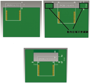
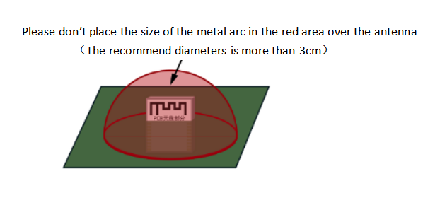
To ensure optimal WiFi performance when the WiFi module uses an onboard PCB antenna, it is recommended that the antenna be at least 15 mm away from other metal parts.
To ensure the antenna performance, the PCB should not be routed or clad with copper in the antenna area.
Antenna Connector Specifications
There is no antenna connector for this module for the moment.
Packaging Information and Production Instructions
Mechanical Dimensions
Specifications of a Terminal
The specifications of the terminal are 2.0 mm*4 Pin. Detailed parameters are as follows:
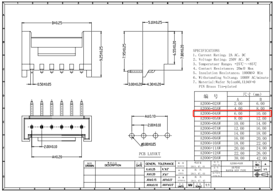
Parameters of the Shell
Production Instructions
Storage conditions for a delivered module are as follows:
1. The moisture-proof bag must be placed in an environment where the temperature is below 30°C and the relative humidity is lower than 85%.
2. The shelf life of a dry-packaged product is 6 months from the date when the product is packaged and sealed.
Caution:
1. In the production process, all operators must wear electrostatic rings.
2. During operation, strictly prevent the module from getting wet or dirty.
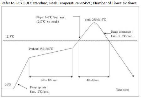
Recommended Oven Temperature Curve
Perform SMT based on the following reflow oven temperature curve. The highest temperature is 245°C. The reflow temperature curve is shown as belows:
Storage conditions

MOQ and Packaging Information
| Product Number | MOQ (pcs) | Shipping packaging method | The number of modules per carton (pcs) | The number of reels per carton (reel) |
|---|---|---|---|---|
| JWBR2S-3.3V | Packaging through bubble bags | 200 | 2 |
Is this page helpful?
YesFeedbackIs this page helpful?
YesFeedback


